ALLPCB


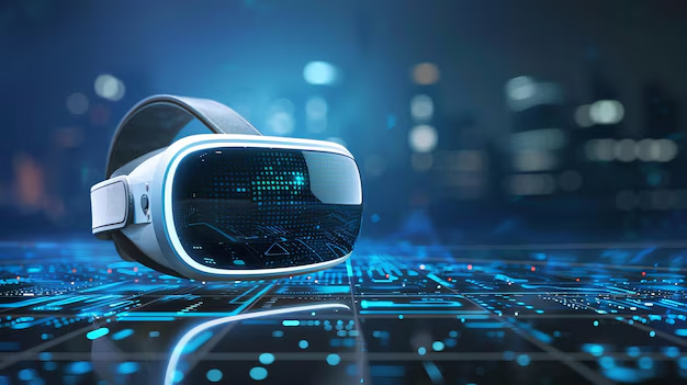
In the fast-evolving world of virtual reality (VR), creating smaller, lighter, and more powerful headsets is a top priority. How can manufacturers achieve this? The answer lies in High-Density Interconnect (HDI) PCBs. These advanced circuit boards are revolutionizing VR headset design with their ability to pack more functionality into tiny spaces. In this blog, we’ll explore how HDI PCB VR headset technology, high-density interconnect VR solutions, microvia technology VR applications, advanced PCB design VR innovations, and miniaturization VR headset trends are shaping the future of immersive experiences.
What Are HDI PCBs and Why Do They Matter for VR?
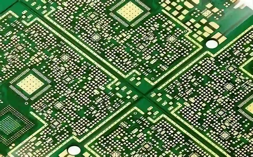
HDI PCBs are specialized circuit boards that use high-density interconnects to fit more components and connections into a smaller area compared to traditional PCBs. They achieve this through finer lines, smaller vias, and advanced layering techniques. For VR headsets, where space is limited and performance is critical, HDI technology is a game-changer.
VR headsets need to process massive amounts of data for high-resolution displays, real-time tracking, and seamless user interactions. HDI PCBs enable this by supporting faster signal transmission and reducing signal loss. With trace widths as small as 3 mils (0.003 inches) and microvias with diameters under 6 mils, these boards can handle the high-speed signals (often exceeding 5 Gbps) required for next-gen VR systems.
The Role of High-Density Interconnect VR in Headset Design
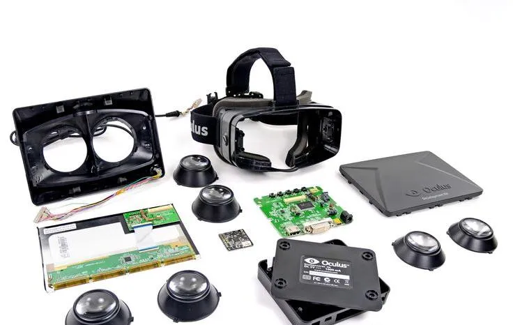
High-density interconnect VR technology is at the heart of modern headset designs. Traditional PCBs often struggle with the space constraints and performance demands of VR devices. HDI PCBs solve this by allowing more layers—sometimes up to 12 or more—in a thinner profile. This means engineers can integrate complex circuits for graphics processing, sensors, and wireless connectivity without increasing the headset's size or weight.
For example, a typical VR headset might require multiple chips for rendering 4K visuals per eye at 90 Hz refresh rates. HDI PCBs can route these high-speed signals with minimal interference, ensuring smooth performance. Additionally, their compact design helps reduce the overall weight of the headset, making it more comfortable for extended use.
Microvia Technology VR: Enabling Miniaturization
Microvia technology VR is a critical component of HDI PCBs. Microvias are tiny holes (often less than 0.006 inches in diameter) drilled into the PCB to connect different layers. Unlike traditional through-hole vias, microvias take up much less space and allow for denser routing. This is essential for miniaturization VR headset designs, where every millimeter counts.
In practical terms, microvias enable VR headsets to shrink in size while maintaining or even improving performance. They support higher component density, meaning more powerful processors, memory chips, and sensors can fit into a smaller footprint. This technology also reduces signal path lengths, cutting down on latency—a key factor for VR where even a 1-millisecond delay can disrupt immersion.
Advanced PCB Design VR: Meeting Complex Challenges
Advanced PCB design VR techniques go hand-in-hand with HDI technology to address the unique challenges of VR hardware. VR headsets must balance power efficiency, thermal management, and signal integrity in a confined space. HDI PCBs, with their fine-pitch traces and stacked layers, are ideal for meeting these demands.
One key aspect of advanced design is impedance control. VR systems often operate at high frequencies, and mismatched impedance can lead to signal reflection and data loss. HDI PCBs can be designed with controlled impedance traces (typically targeting 50 ohms for high-speed signals) to ensure reliable performance. Additionally, the use of buried and blind vias in HDI boards helps optimize space and maintain signal integrity by reducing crosstalk between layers.
Thermal management is another critical area. VR headsets generate significant heat due to intensive processing. HDI PCBs can incorporate thermal vias and heat-dissipating materials to manage temperatures, preventing overheating during long sessions. For instance, some designs use copper-filled microvias to transfer heat away from critical components, maintaining operational stability.
Miniaturization VR Headset: Why Size Matters
Miniaturization VR headset trends are driving the industry forward, and HDI PCBs are the backbone of this movement. Smaller, lighter headsets are not just more comfortable—they also open up new possibilities for portable and standalone VR systems. Users no longer want bulky devices tethered to powerful PCs; they demand sleek, wireless headsets with built-in computing power.
HDI PCBs make this possible by shrinking the electronic footprint. A standalone VR headset, for instance, might integrate a high-performance GPU, battery management system, and multiple sensors into a single compact board. This level of integration cuts down on wiring and connectors, reducing weight and potential failure points. Some modern headsets weigh as little as 300 grams, thanks in large part to HDI-driven miniaturization.
Benefits of HDI PCBs for VR Headset Manufacturers
For manufacturers, adopting HDI PCB VR headset technology offers several advantages. First, it allows for faster product development cycles. With HDI boards, engineers can prototype and test complex designs more efficiently, reducing time-to-market for next-gen headsets.
Second, HDI PCBs improve reliability. Their advanced construction techniques, such as laser-drilled microvias and high-quality laminates, result in boards that withstand the rigors of daily use. This is crucial for VR headsets, which often endure frequent handling and varying environmental conditions.
Finally, HDI technology supports cost-effective scaling. While the initial design and manufacturing of HDI PCBs may be more complex, the ability to integrate more functions into a single board reduces the need for multiple components and assemblies. Over time, this can lower production costs, especially for high-volume runs.
Challenges in Implementing HDI PCBs for VR
While HDI PCBs offer immense benefits, they come with challenges that manufacturers must navigate. One major hurdle is the complexity of design and fabrication. Creating boards with microvias and fine traces requires specialized software, skilled engineers, and advanced manufacturing equipment. Even a small error in layer alignment or via placement can lead to signal issues or board failure.
Another challenge is cost. HDI PCBs are generally more expensive to produce than traditional boards due to the materials and precision involved. For VR headset makers targeting budget-conscious consumers, this can be a limiting factor. However, as HDI technology becomes more widespread, costs are gradually decreasing, making it accessible to a broader market.
Lastly, testing and quality assurance are critical. VR headsets rely on flawless performance, and HDI PCBs must undergo rigorous testing to ensure signal integrity, thermal stability, and durability. Manufacturers need to invest in advanced testing protocols to catch potential issues before products reach the market.
Future Trends: HDI PCBs and the Evolution of VR
Looking ahead, the role of HDI PCBs in VR is only set to grow. As VR technology advances, headsets will demand even higher performance in smaller packages. Emerging trends like 8K resolution per eye, eye-tracking, and foveated rendering will require PCBs capable of handling unprecedented data rates—potentially exceeding 10 Gbps per channel.
HDI technology is also evolving to meet these needs. Innovations like stacked microvias and ultra-thin dielectrics are pushing the boundaries of what’s possible, enabling even denser and more efficient designs. Additionally, the integration of flexible and rigid-flex HDI boards could lead to headsets with foldable or modular components, further enhancing portability.
Beyond hardware, HDI PCBs will play a role in supporting software-driven VR features. As artificial intelligence and machine learning become integral to VR experiences, headsets will need onboard processing power for real-time data analysis. HDI PCBs can accommodate the compact, high-speed chips required for these applications, paving the way for smarter, more immersive devices.
How to Get Started with HDI PCBs for VR Projects
For engineers and manufacturers looking to incorporate HDI PCBs into VR headset designs, the first step is partnering with a reliable PCB provider. Look for a partner with experience in high-density interconnect VR solutions and a track record of delivering precise, high-quality boards.
Next, invest in design tools that support HDI layouts. Software with advanced routing and simulation capabilities can help optimize trace placement, via structures, and impedance control. Collaboration between design and manufacturing teams is also essential to ensure that the board’s specifications align with production capabilities.
Finally, prioritize iterative testing. Build prototypes, simulate real-world VR workloads, and analyze performance metrics like signal latency and thermal behavior. Refining the design based on test data will result in a more robust and efficient final product.
Conclusion: Powering the Future of VR with HDI PCBs
HDI PCBs are transforming the VR industry by enabling smaller, faster, and more powerful headsets. Through high-density interconnect VR technology, microvia technology VR innovations, advanced PCB design VR strategies, and miniaturization VR headset trends, manufacturers can meet the growing demands of immersive tech users. While challenges like design complexity and cost remain, the benefits of HDI PCBs—compact size, enhanced performance, and scalability—make them indispensable for next-gen VR devices.
At ALLPCB, we’re committed to supporting the VR revolution with cutting-edge HDI PCB solutions. Whether you’re designing a lightweight standalone headset or pushing the limits of visual fidelity, our expertise and manufacturing capabilities can help bring your vision to life. Embrace the future of VR with HDI technology and create experiences that captivate and inspire.