 ALLPCB


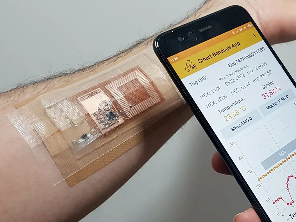
In the rapidly evolving world of wearable health technology, designing a flexible PCB (Printed Circuit Board) is a game-changer. Whether you're exploring flexible PCB DIY projects or diving into wearable electronics design, mastering the art of building flex circuits can unlock innovative solutions for health monitoring devices. This guide by ALLPCB dives deep into advanced techniques for creating flexible PCBs tailored for wearable health applications. We'll cover everything from choosing the right flex PCB materials to executing advanced PCB projects, ensuring you have the knowledge to bring your ideas to life.
What Are Flexible PCBs and Why Use Them in Wearable Health Devices?
Flexible PCBs are thin, lightweight circuit boards that can bend and conform to various shapes without breaking. Unlike rigid PCBs, they are made from pliable materials, allowing them to fit into compact, irregular spaces. In wearable health applications—think fitness trackers, smartwatches, or medical patches—flexible PCBs are essential. They provide comfort by adapting to the body's contours, reduce device weight, and enable innovative designs that rigid boards can't achieve.
The demand for wearable health devices is soaring. According to industry data, the global wearable medical device market is expected to grow at a compound annual growth rate (CAGR) of over 20% from 2023 to 2030. Flexible PCBs are at the heart of this growth, enabling smaller, more durable, and user-friendly products. Let’s explore how to create these circuits using advanced techniques.
Understanding Flex PCB Materials for Wearable Health Applications
Choosing the right flex PCB materials is the foundation of any successful design. The materials must balance flexibility, durability, and biocompatibility since wearable health devices often come into direct contact with skin. Here are the key materials to consider:
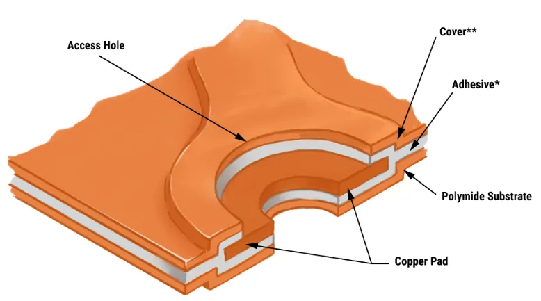
- Substrate Materials: Polyimide (PI) is the most common substrate for flexible PCBs due to its excellent thermal stability and flexibility. It can withstand temperatures up to 400°C, making it ideal for soldering processes. Polyester (PET) is another option, often used for lower-cost applications, though it has lower heat resistance.
- Conductive Layers: Copper is the standard choice for conductive traces in flex circuits due to its high conductivity and flexibility. Rolled annealed (RA) copper is preferred over electrodeposited (ED) copper because it offers better flexibility and fatigue resistance, crucial for repeated bending in wearables.
- Coverlay and Adhesives: A coverlay, often made of polyimide with an adhesive layer, protects the circuit while maintaining flexibility. Silicone-based adhesives are sometimes used for their biocompatibility in health applications.
- Finishes: For wearable devices, surface finishes like immersion gold or organic solderability preservatives (OSP) are used to prevent oxidation and ensure reliable connections. These finishes must also be non-toxic and skin-safe.
When selecting materials, consider the specific requirements of your wearable health device. For instance, a heart rate monitor may need materials with high signal integrity to avoid interference, targeting impedance values around 50 ohms for optimal performance.
Key Design Considerations for Wearable Electronics Design
In wearable electronics design, creating a flexible PCB requires careful planning to ensure functionality, durability, and user comfort. Here are critical design considerations:
1. Bend Radius and Flexibility
The bend radius—the minimum radius a flex PCB can be bent without damage—is crucial. A typical guideline is to maintain a bend radius of at least 10 times the thickness of the board for dynamic bending (repeated flexing). For a 0.1 mm thick board, aim for a bend radius of 1 mm or more. Over-bending can cause trace cracking or delamination, so design with the end-use in mind, such as a wristband that flexes repeatedly.
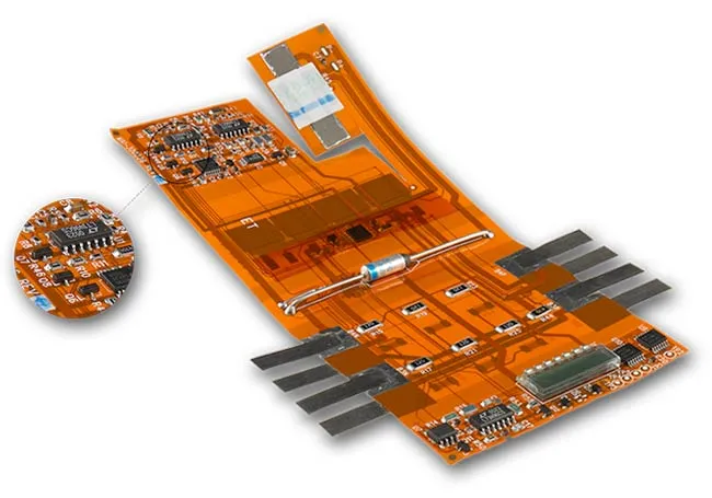
2. Layer Stack-Up
Flexible PCBs often have 1 to 4 layers for wearable applications. Minimize the number of layers to keep the board thin and flexible. Place critical signal traces on inner layers to protect them from stress, and use staggered vias to reduce strain points. For high-speed signals in health sensors, maintain controlled impedance, often around 50-100 ohms, depending on the application.
3. Component Placement
Place components in areas that experience minimal bending to avoid stress on solder joints. Use lightweight, low-profile components like 0201 or 0402 SMD (surface-mount device) packages to reduce bulk in wearable designs. Reinforce component areas with stiffeners if needed, especially for connectors or ICs.
4. Biocompatibility and Safety
Since wearable health devices contact skin, ensure all materials are biocompatible and comply with standards like ISO 10993 for medical devices. Avoid materials that could cause irritation or allergic reactions, and test for long-term wear safety.
Advanced Techniques for Building Flex Circuits
Building flex circuits for wearable health applications involves advanced techniques to ensure precision and reliability. Here’s a step-by-step approach:
1. Prototyping with Simulation Tools
Before manufacturing, use simulation software to test your design for mechanical stress and signal integrity. Tools can predict how the PCB will behave under bending and identify potential failure points. For example, simulate a signal speed of 1 GHz for a health sensor to ensure data accuracy without interference.
2. Precision Etching for Fine Traces
Wearable devices often require fine traces (as small as 50 micrometers) to fit complex circuits into small spaces. Use advanced photo-etching processes to achieve high precision, ensuring clean edges and consistent trace widths for reliable signal transmission.
3. Dynamic Flex Testing
After fabrication, subject the flex PCB to dynamic flex testing to simulate real-world use. Test for at least 10,000 bend cycles at the expected bend radius to ensure durability. This is critical for health devices like smart patches that must endure constant movement.
4. Integration of Sensors and Antennas
Many wearable health devices rely on sensors (e.g., temperature, heart rate) and antennas for wireless communication. Embed these directly into the flex PCB to save space. Use conductive inks or thin-film technologies for antennas to maintain flexibility, targeting a signal range of 2.4 GHz for Bluetooth connectivity.
Flexible PCB DIY: Tips for Hobbyists and Engineers
For those exploring flexible PCB DIY projects, creating a flex circuit at home or in a small lab is possible with the right approach. While professional manufacturing offers precision, DIY enthusiasts can start small with these tips:
- Start with Simple Designs: Begin with a single-layer flex PCB design for a basic wearable like a step counter. Use open-source design software to create your layout, focusing on larger traces (e.g., 0.2 mm width) to avoid etching errors.
- Use DIY Materials: Purchase thin polyimide films and copper foil from online suppliers. Laminate them using heat and pressure with a household iron, then etch the copper using ferric chloride solution for trace patterns.
- Test with Low-Cost Tools: Use a multimeter to check continuity and resistance (aim for under 1 ohm per trace) after etching. Bend the board manually to test flexibility, ensuring no cracks form after 50-100 bends.
- Safety First: Wear gloves and work in a ventilated area when handling chemicals for etching. Ensure your DIY flex PCB materials are safe for skin contact if used in wearables.
While DIY is great for learning, partnering with a professional manufacturer like ALLPCB ensures high-quality results for complex advanced PCB projects, especially for medical-grade wearables.
Challenges in Flexible PCB Design for Wearable Health Devices
Designing flexible PCBs for health applications comes with unique challenges. Understanding these can help you avoid costly mistakes:
- Signal Integrity: Flex circuits are prone to noise and crosstalk due to their thin structure. Use ground planes and proper trace spacing (e.g., 0.1 mm minimum) to minimize interference, especially for high-speed signals above 500 MHz.
- Durability Under Stress: Repeated bending can cause fatigue failure. Reinforce high-stress areas with additional coverlay or adhesive layers to extend lifespan beyond 50,000 bend cycles.
- Cost Constraints: Flex PCBs are often more expensive to produce than rigid boards due to specialized materials and processes. Optimize your design by minimizing layers and using standard material thicknesses (e.g., 0.05 mm polyimide) to control costs.
Future Trends in Flex PCBs for Wearable Health Technology
The future of flexible PCBs in wearable health tech is exciting. Innovations like stretchable electronics, where circuits can elongate by up to 30% without damage, are on the horizon. Conductive inks and 3D printing are also emerging, allowing for fully customized, lightweight designs. Additionally, integration of AI-driven sensors into flex PCBs will enable real-time health data analysis with signal processing speeds exceeding 1 GHz.
At ALLPCB, we’re committed to staying at the forefront of these advancements, providing cutting-edge solutions for your advanced PCB projects. Whether you're a hobbyist or a professional engineer, leveraging these trends can position you as a leader in wearable health innovation.
Conclusion: Mastering Flexible PCBs for Wearable Health Applications
Creating a flexible PCB for wearable health applications is a rewarding challenge that blends creativity with technical precision. By understanding flex PCB materials, mastering wearable electronics design, and applying advanced techniques for building flex circuits, you can develop innovative devices that improve lives. Whether you’re experimenting with flexible PCB DIY or tackling advanced PCB projects, the key is to prioritize durability, biocompatibility, and user comfort.
ALLPCB is here to support your journey with high-quality manufacturing services tailored to flexible PCB needs. Start small, test often, and scale your designs with confidence. The future of wearable health technology is flexible—bend the rules of innovation today!


