 ALLPCB


When designing a printed circuit board (PCB), one of the most critical decisions you'll make is selecting the right type of via. Vias are small conductive paths that connect different layers of a PCB, ensuring electrical signals can travel seamlessly. But not all vias are the same. Choosing between options like through-hole via vs blind via vs buried via, or deciding on advanced solutions like microvias or stacked vias, can significantly impact your design's performance, reliability, and cost. In this comprehensive guide, we'll break down the different via types, their fabrication processes, design considerations, reliability factors, and costs to help you make an informed decision for your next project.
Whether you're working on a simple single-layer board or a complex multilayer design, understanding via types is essential. Let's dive into the details of each via type, explore their applications, and provide actionable insights to optimize your PCB design.
What Are Vias in PCB Fabrication?
Vias, short for Vertical Interconnect Access, are small holes drilled or formed in a PCB to create electrical connections between layers. These connections are typically plated with conductive material, like copper, to allow signals or power to pass through. Vias are indispensable in multilayer PCBs, where components and traces on different layers need to communicate. The type of via you choose depends on factors like board complexity, space constraints, signal integrity requirements, and budget.
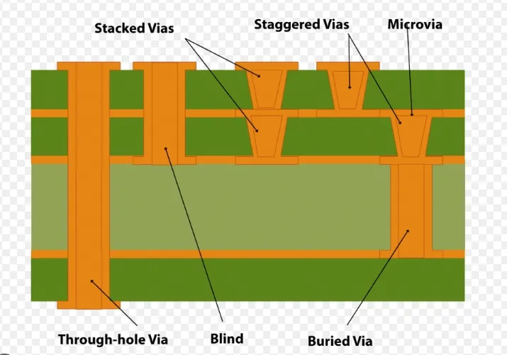
There are several types of vias used in PCB fabrication, each with unique characteristics. Below, we'll explore the most common ones—through-hole, blind, buried, and microvias—along with specialized options like via-in-pad and stacked vias.
Through-Hole Via vs Blind Via vs Buried Via: Understanding the Basics
Let’s start with the fundamental via types and compare their features, applications, and limitations. This comparison of through-hole via vs blind via vs buried via will help you determine which suits your design needs.
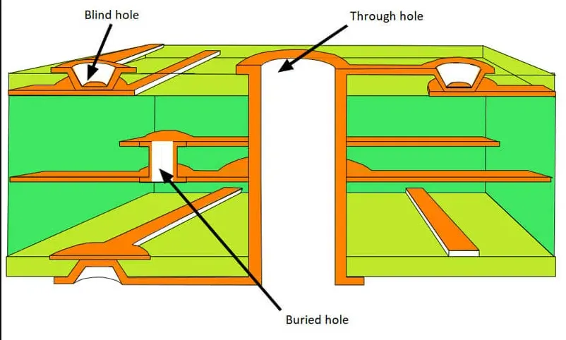
Through-Hole Via
Through-hole vias are the most traditional and widely used type. They extend through the entire thickness of the PCB, connecting the top layer to the bottom layer and all layers in between. These vias are mechanically drilled and plated with copper to ensure conductivity.
- Advantages: Simple to fabricate, cost-effective, and highly reliable for basic designs. They can handle higher current due to their larger size (typically 0.2-0.8 mm in diameter).
- Disadvantages: They take up space on all layers, limiting routing options in high-density designs. They can also introduce parasitic capacitance, affecting high-speed signals (above 1 GHz).
- Applications: Ideal for single- or double-layer boards, power electronics, and designs where space isn’t a major constraint.
Blind Via
Blind vias connect an outer layer (top or bottom) to one or more inner layers but do not extend through the entire board. They are often formed using laser drilling for precision, especially in smaller sizes.
- Advantages: Saves space on the opposite outer layer, allowing for more component placement or routing. Reduces signal interference compared to through-hole vias.
- Disadvantages: More complex and costly to fabricate due to precise drilling requirements. Limited to connecting specific layers, which may require additional vias for full connectivity.
- Applications: Common in high-density interconnect (HDI) designs and multilayer boards where space optimization is critical.
Buried Via
Buried vias are located entirely within the inner layers of a PCB and do not reach the outer surfaces. Like blind vias, they are often created using laser drilling or controlled-depth mechanical drilling.
- Advantages: Frees up space on both outer layers for components and traces. Enhances signal integrity by reducing stub effects in high-speed designs (up to 10 GHz or more).
- Disadvantages: Expensive to manufacture due to the complexity of drilling and plating within internal layers. Harder to inspect or repair if issues arise.
- Applications: Used in advanced HDI designs, smartphones, and compact electronics where layer-to-layer connectivity must be optimized without affecting surface space.
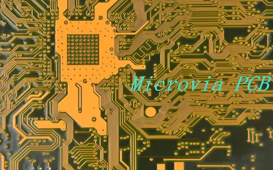
Microvia Fabrication Process: Precision for High-Density Designs
Microvias are small-diameter vias, typically less than 0.15 mm, used in HDI PCBs to achieve greater routing density. The microvia fabrication process involves advanced techniques to ensure precision and reliability.
Steps in Microvia Fabrication:
- Laser Drilling: Unlike traditional mechanical drilling, microvias are created using laser technology for high precision. This allows for smaller holes with aspect ratios (depth-to-diameter) often below 1:1, ensuring better signal integrity.
- Cleaning: Post-drilling, the holes are cleaned to remove debris or residue that could affect plating.
- Plating: A thin layer of copper is deposited inside the microvia using electroless plating, followed by electroplating to build up the conductive layer.
- Inspection: Microvias are inspected for connectivity and structural integrity, often using automated optical inspection (AOI) systems.
Benefits: Microvias enable finer pitch components (down to 0.4 mm or less), reduce layer count in some designs, and support high-speed signals (up to 25 GHz in advanced applications).
Challenges: The microvia fabrication process is more expensive and requires specialized equipment. Reliability can be a concern if not designed with proper aspect ratios or if thermal stresses are not accounted for during assembly.
Via-in-Pad Design Considerations: Balancing Space and Performance
Via-in-pad is a design technique where a via is placed directly within the pad of a surface-mount component, such as a ball grid array (BGA). This approach is often used in HDI designs to save space and improve routing efficiency.
Key Design Considerations:
- Solder Wicking: During reflow soldering, solder can flow into the via, leading to insufficient solder on the pad. To prevent this, vias are often filled with conductive or non-conductive material and capped with a planar surface (via plugging).
- Thermal Management: Vias in pads can act as heat sinks, potentially causing uneven heating during assembly. Designers must ensure proper thermal relief or filling to mitigate this.
- Signal Integrity: For high-speed designs, via-in-pad can reduce trace length and improve signal performance, but care must be taken to avoid impedance mismatches (target impedance often around 50 ohms for digital signals).
- Fabrication Complexity: Via-in-pad requires additional steps like filling and planarization, increasing manufacturing costs by approximately 10-20% compared to standard vias.
Applications: Widely used in compact devices with BGAs or fine-pitch components where traditional via placement would consume too much space.
Stacked Via Reliability: Ensuring Long-Term Performance
Stacked vias are multiple vias aligned vertically on top of each other across different layers, often used in HDI designs to connect several layers in a compact space. While they save space and improve routing, stacked via reliability is a critical concern.
Factors Affecting Reliability:
- Thermal Stress: During soldering or operation, thermal expansion can cause cracks or delamination in stacked vias, especially if the aspect ratio exceeds 1:1. Using filled vias can reduce this risk by up to 30% based on industry testing.
- Alignment Accuracy: Misalignment during fabrication can lead to poor connectivity. Advanced laser drilling and imaging systems help achieve alignment tolerances within 0.05 mm.
- Material Selection: Choosing materials with matching coefficients of thermal expansion (CTE) for the PCB substrate and via fill can enhance reliability under temperature cycles (-40°C to 125°C in typical applications).
Best Practices: Limit the number of stacked vias to 2-3 per connection in most designs to minimize stress. Opt for staggered vias (offset rather than directly stacked) if reliability is a higher priority than density.
Cost of Different Via Types: Balancing Budget and Performance
The cost of different via types varies significantly based on fabrication complexity, equipment requirements, and design specifications. Here's a breakdown to help you weigh cost against performance:
- Through-Hole Vias: Lowest cost, often less than $0.01 per via in high-volume production. Simple mechanical drilling and plating keep expenses down, making them ideal for budget-conscious projects.
- Blind Vias: Moderately expensive, with costs ranging from $0.05 to $0.10 per via due to controlled-depth drilling or laser processes. Costs increase with tighter tolerances or smaller diameters.
- Buried Vias: Similar to blind vias in cost ($0.05 to $0.10 per via) but can be higher if multiple internal layers are involved. Fabrication complexity drives up the price.
- Microvias: Among the priciest, costing $0.10 to $0.20 per via or more, due to laser drilling and precise plating requirements. However, they can reduce overall board cost by minimizing layer count.
- Stacked Vias: Costs can stack up (pun intended) to $0.15 to $0.30 per connection, reflecting the multiple vias and alignment challenges. Often reserved for high-end designs.
- Via-in-Pad: Adds an extra 10-20% to standard via costs due to filling and planarization processes, but can save on overall board size, offsetting the expense in compact designs.
Cost-Saving Tip: Evaluate your design needs carefully. For instance, combining through-hole vias for power connections with blind or microvias for signal routing can optimize both cost and performance.
How to Choose the Right Via for Your PCB Design
Selecting the appropriate via type involves balancing several factors. Here’s a step-by-step approach to guide your decision:
- Determine Design Complexity: For simple, low-density designs, through-hole vias are often sufficient. For HDI or multilayer boards, consider blind, buried, or microvias.
- Assess Signal Requirements: High-speed signals (above 1 GHz) benefit from microvias or buried vias to minimize interference and stub effects.
- Consider Space Constraints: If surface space is limited, via-in-pad or stacked vias can help maximize routing and component placement.
- Evaluate Budget: Weigh the cost of different via types against the project budget. Sometimes, investing in advanced vias can reduce overall costs by shrinking board size or layer count.
- Focus on Reliability: For applications with harsh environmental conditions (e.g., automotive or aerospace), prioritize via types and designs with proven reliability, like filled or staggered vias over stacked ones.
Conclusion: Optimize Your PCB Design with the Right Via
Choosing the right via type is a cornerstone of effective PCB design. Whether you're comparing through-hole via vs blind via vs buried via, exploring the microvia fabrication process, considering via-in-pad design considerations, evaluating stacked via reliability, or analyzing the cost of different via types, each decision impacts your board’s performance and manufacturability. By understanding the strengths and limitations of each via type, you can create designs that meet technical requirements while staying within budget.
At ALLPCB, we’re committed to supporting your PCB projects with high-quality fabrication and expert guidance. Use this guide as a starting point to select the best vias for your design, ensuring efficiency, reliability, and cost-effectiveness in every layer of your board.


