 ALLPCB


If you're a PCB engineer looking to understand the ins and outs of V-scoring, you've come to the right place. V-scoring, also known as PCB V-scoring, is a manufacturing technique used to create grooves on a printed circuit board (PCB) panel, making it easier to separate individual boards without damage. In this detailed guide, we'll explore the PCB V-scoring process, design rules, advantages, disadvantages, costs, and tolerances to help you make informed decisions for your projects.
Whether you're optimizing a high-volume production run or designing a prototype, mastering V-scoring can save time, reduce costs, and improve the quality of your boards. Let’s dive into everything you need to know about this essential PCB manufacturing method.
What is PCB V-Scoring?
V-scoring is a process where a V-shaped groove is cut into the surface of a PCB panel using specialized machinery. This groove weakens the material along a specific line, allowing engineers or manufacturers to snap the panel into individual boards after assembly. Typically, the groove is cut on both the top and bottom sides of the panel, leaving a thin strip of material (often called the "web") in the middle that holds the boards together until they are ready to be separated.
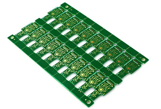
This method is widely used in PCB manufacturing, especially when producing multiple boards on a single panel. It’s a cost-effective and efficient way to handle depaneling, which is the process of separating individual PCBs from a larger panel. Understanding the PCB V-scoring process is crucial for engineers who want to ensure clean breaks and maintain the integrity of their designs.
The PCB V-Scoring Process: How It Works
The PCB V-scoring process involves several key steps that ensure precision and reliability. Here's a breakdown of how it’s done:
- Design Preparation: Engineers specify the V-score lines in their PCB design files, indicating where the panel should be separated into individual boards. These lines must align with the board's layout to avoid damaging components or traces.
- Panel Fabrication: During manufacturing, the PCB panel is created with multiple boards arranged together. The panel material is typically a standard FR-4 or similar substrate.
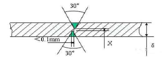
- Scoring: A specialized scoring machine equipped with a V-shaped blade cuts grooves into the panel along the designated lines. The blade typically cuts at a 30-degree or 45-degree angle, penetrating about one-third of the board thickness on each side, leaving a small web of material (often 0.3 to 0.5 mm thick) in the center.
- Assembly: Components are mounted on the panel while the boards are still connected. This allows for efficient handling during soldering and testing.
- Depaneling: Once assembly and testing are complete, the panel is manually or mechanically snapped along the V-score lines to separate the individual boards.
The precision of the scoring machine is critical. A deviation of even 0.1 mm can lead to uneven breaks or damage to nearby traces. Therefore, working with a reliable manufacturing partner is essential to ensure consistent results in the PCB V-scoring process.
V-Scoring Design Rules: Key Guidelines for Engineers
Following V-scoring design rules is vital to achieving clean separations and avoiding issues during manufacturing. Here are the most important guidelines to keep in mind:
- Minimum Board Thickness: V-scoring is typically suitable for boards with a thickness of 0.6 mm to 2.0 mm. Thinner boards may crack during scoring, while thicker boards might not snap cleanly.
- Web Thickness: The remaining web of material between the top and bottom grooves should be about one-third of the board thickness, usually between 0.3 mm and 0.5 mm. This ensures the panel holds together during assembly but can still be snapped apart easily.
- Component Placement: Keep components, traces, and vias at least 1.0 mm away from the V-score line to prevent damage during separation. For high-density designs, a clearance of 1.5 mm is safer.
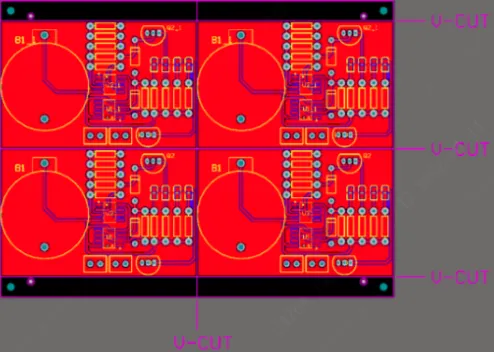
- Score Line Alignment: V-score lines must be straight and continuous. Curved or angled lines are not suitable for this method and may require alternative depaneling techniques like routing.
- Panel Edge Clearance: Maintain a minimum distance of 5.0 mm between the V-score line and the panel’s outer edge to ensure stability during handling.
- Material Compatibility: V-scoring works best with standard materials like FR-4. For flexible or rigid-flex PCBs, consult your manufacturer, as scoring may not be appropriate.
Adhering to these V-scoring design rules helps minimize manufacturing defects and ensures that your boards separate cleanly without compromising structural integrity.
V-Scoring Advantages: Why Choose This Method?
V-scoring offers several benefits that make it a popular choice for PCB engineers. Here’s why you might consider it for your next project:
- Cost-Effective: V-scoring is one of the most economical depaneling methods, especially for high-volume production. It reduces the need for complex tooling or additional processing steps, keeping the overall V-scoring cost low.
- High Efficiency: Scoring allows multiple boards to be processed as a single panel during assembly, streamlining soldering, testing, and inspection. This can cut production time by up to 30% compared to handling individual boards.
- Clean Separation: When done correctly, V-scoring results in smooth edges with minimal stress on the board, reducing the risk of delamination or cracking.
- Scalability: This method is ideal for both small prototype runs and large-scale manufacturing, offering flexibility for projects of any size.
- Reduced Equipment Wear: Unlike routing, which uses high-speed cutting tools that wear out quickly, V-scoring relies on simpler blades that have a longer lifespan, further lowering costs.
These V-scoring advantages make it a go-to option for engineers looking to balance quality and budget in their PCB designs.
V-Scoring Disadvantages: Challenges to Consider
While V-scoring has many benefits, it’s not without its drawbacks. Understanding these V-scoring disadvantages can help you decide if it’s the right method for your project:
- Limited to Straight Lines: V-scoring can only be applied in straight lines. If your design requires complex shapes or curves for separation, you’ll need to use a different depaneling method like milling or laser cutting.
- Risk of Stress Damage: Improper scoring depth or web thickness can cause stress during separation, leading to cracks or damage near the score line. This risk increases with thinner boards (below 0.6 mm).
- Not Suitable for All Materials: V-scoring is less effective on flexible PCBs or materials with high tensile strength, as they may not snap cleanly or could deform during the process.
- Edge Roughness: Although V-scoring generally produces clean edges, slight roughness or burrs can occur, especially if the scoring blade is dull or misaligned. This may require additional finishing steps for high-precision applications.
- Component Proximity Issues: If components are placed too close to the score line, they risk being damaged during separation, limiting design flexibility in high-density layouts.
Being aware of these V-scoring disadvantages allows engineers to weigh the pros and cons and choose the best depaneling method for their specific needs.
V-Scoring Cost: What to Expect
The V-scoring cost is generally lower than other PCB depaneling methods, making it an attractive option for many projects. However, the exact cost depends on several factors:
- Panel Size and Complexity: Larger panels with more score lines require more machine time, increasing costs. A standard panel of 200 mm x 300 mm with 10 score lines might cost an additional $5 to $10 for scoring.
- Board Thickness: Thicker boards may need deeper or wider grooves, which can slightly raise the cost due to additional machine setup or blade wear.
- Volume: High-volume orders often benefit from economies of scale, reducing the per-unit cost of V-scoring. For example, scoring a single prototype panel might cost $10, while the cost per panel in a 1,000-unit run could drop to $2 or less.
- Manufacturer Capabilities: Some manufacturers include V-scoring as part of their standard panelization service at no extra charge, while others may charge a setup fee for custom scoring configurations.
On average, V-scoring adds a minimal cost to the overall PCB production budget, often ranging from $0.50 to $5 per panel for standard designs. For engineers, this affordability is a key reason to consider V-scoring over more expensive alternatives like laser cutting, which can cost $20 or more per panel.
V-Scoring Tolerances: Precision Matters
V-scoring tolerances refer to the acceptable deviation in the depth, width, and alignment of the grooves. Tight tolerances are essential for ensuring clean breaks and preventing damage. Here are the typical V-scoring tolerances to keep in mind:
- Depth Tolerance: The depth of the groove should be within ±0.05 mm of the specified value. For a 1.6 mm thick board, the groove depth on each side might be 0.5 mm, leaving a 0.6 mm web. Deviations beyond this range can cause uneven snapping.
- Alignment Tolerance: The alignment of the V-score line should be accurate to within ±0.1 mm. Misalignment can result in grooves cutting into critical areas of the board, damaging traces or components.
- Web Thickness Tolerance: The remaining web thickness should be consistent across the panel, with a tolerance of ±0.05 mm. Inconsistent web thickness can lead to some boards snapping too easily while others require excessive force.
- Blade Angle: The angle of the V-cut (typically 30 or 45 degrees) must be uniform to ensure consistent stress distribution during separation.
Manufacturers with advanced equipment can achieve tighter V-scoring tolerances, often down to ±0.03 mm for high-precision applications. As an engineer, it’s important to specify your tolerance requirements clearly in the design files to avoid issues during production.
Best Practices for Implementing V-Scoring in Your Designs
To maximize the benefits of V-scoring and avoid common pitfalls, follow these best practices:
- Collaborate with Your Manufacturer: Early communication with your manufacturing partner can help identify potential issues with V-scoring in your design. Provide detailed documentation of score line locations and tolerances.
- Test with Prototypes: For critical projects, order a small batch of panels with V-scoring to test the separation process. This can help you fine-tune web thickness and clearance distances before full-scale production.
- Use Design Software Features: Most PCB design tools allow you to define V-score lines in the panelization stage. Take advantage of these features to ensure accurate placement and alignment.
- Plan for Post-Separation Finishing: If edge smoothness is critical for your application, budget for light sanding or other finishing processes after depaneling to remove any minor burrs.
- Consider Alternative Methods if Needed: If V-scoring isn’t suitable due to material type or design complexity, explore other options like tab routing or laser depaneling for better results.
By incorporating these practices, you can ensure a smoother manufacturing process and higher-quality PCBs.
Conclusion: Mastering V-Scoring for Better PCB Designs
V-scoring is a powerful and cost-effective technique for PCB depaneling, offering numerous advantages for engineers working on projects of all sizes. By understanding the PCB V-scoring process, adhering to V-scoring design rules, and carefully weighing the V-scoring advantages and disadvantages, you can make informed decisions that enhance the efficiency and quality of your designs.
Keep in mind the V-scoring cost and tolerances when planning your project budget and specifications. With the right approach, this method can help you achieve clean, reliable separations while minimizing production expenses. Whether you're designing a simple prototype or a complex multi-board panel, V-scoring is a tool worth mastering.
At ALLPCB, we’re committed to supporting engineers with the resources and expertise needed to succeed in every stage of PCB development. Explore our services to see how we can help bring your designs to life with precision and efficiency.


