 ALLPCB


When designing digital circuits, one of the most critical decisions is selecting the right PCB trace width. For electronic hobbyists and professionals alike, trace width directly impacts signal integrity, heat dissipation, and overall circuit performance. Whether you're working on a simple microcontroller project or a complex high-speed design, understanding how to choose the appropriate trace width for digital circuits can make or break your project. In this guide, we'll dive deep into the factors that influence PCB trace width in digital circuit design, offering practical tips and detailed insights to help you create reliable and efficient circuit boards.
Why PCB Trace Width Matters in Digital Circuit Design
In digital circuits, PCB traces act as the pathways for electrical signals to travel between components. The width of these traces isn't just a random choice—it affects how well signals are transmitted and how much current the trace can handle without overheating. For digital circuit design trace width, getting it right ensures that your signals remain clear and free from interference, especially in high-speed applications where timing is everything.
Trace width also plays a role in managing heat. If a trace is too narrow for the current it carries, it can overheat, leading to potential damage or failure. On the other hand, overly wide traces can waste valuable board space and complicate the PCB layout for digital designs. Striking the right balance is key, and this blog will walk you through the process step by step.
Factors to Consider When Choosing PCB Trace Width for Digital Circuits
Selecting the right circuit board trace width isn't a one-size-fits-all task. Several factors come into play, especially when designing for digital circuits. Let's break down the most important considerations.
1. Current Carrying Capacity
The amount of current a trace needs to carry is a primary factor in determining its width. Wider traces can handle more current because they have a larger cross-sectional area, which reduces resistance and heat buildup. For digital circuits, most signals carry low current, but power lines or traces connected to high-current components like motors or LEDs may require wider traces.
As a general rule, you can use online calculators or industry standards like the IPC-2221 guidelines to determine the minimum trace width based on current. For example, a trace carrying 1 amp of current on a standard 1 oz copper layer (common in most PCBs) typically needs to be at least 10-15 mils (0.010-0.015 inches) wide to avoid overheating, assuming a temperature rise of 10°C. For digital signals with minimal current, traces as narrow as 6-8 mils may suffice.
2. Signal Integrity in High-Speed Digital Circuits
In high-speed digital circuits, trace width affects signal integrity due to impedance. Impedance is the resistance to the flow of alternating current signals, and mismatched impedance can cause signal reflections, leading to data errors. For high-speed designs like USB, HDMI, or DDR memory interfaces, maintaining controlled impedance is crucial. This often requires specific trace widths and spacing, calculated based on the PCB material's dielectric constant and layer stack-up.
For instance, a 50-ohm impedance trace, common in many high-speed digital applications, might require a width of around 10 mils on a standard FR-4 substrate with a 1.6mm board thickness. Tools like impedance calculators or simulation software can help determine the exact width for your design.
3. Board Space and Layout Constraints
Digital circuit boards often have limited space, especially in compact designs like wearables or IoT devices. Narrower traces allow for denser layouts, but they must still meet current and impedance requirements. Balancing trace width with available space is a common challenge in PCB layout for digital projects. A good practice is to prioritize wider traces for power and ground lines while using narrower traces for low-current signal lines.
4. Manufacturing Capabilities
Not all fabrication houses can produce extremely narrow traces. Standard manufacturing processes often have a minimum trace width of 6 mils, though advanced processes can go as low as 3 mils. Before finalizing your design, confirm the capabilities of your chosen manufacturer to avoid issues during production. For electronic hobbyists working on DIY projects, sticking to wider traces (8-10 mils) can make the design more forgiving and easier to produce.
How to Calculate PCB Trace Width for Digital Circuits
Calculating the right trace width for your digital circuit doesn't have to be complicated. Here's a step-by-step approach to help you get started.
Step 1: Determine Current Requirements
First, identify the maximum current that will flow through each trace. For digital signals, this is often very low (a few milliamps), but power traces may carry several amps. Use a trace width calculator or refer to standards like IPC-2221 to find the minimum width based on current and copper thickness. For example, a 0.5 amp current on a 1 oz copper layer typically requires a trace width of about 7-8 mils for a 10°C temperature rise.
Step 2: Check for Impedance Requirements
If you're designing high-speed digital circuits, calculate the required trace width for controlled impedance. This depends on the characteristic impedance (e.g., 50 ohms for many high-speed signals), the PCB material, and the layer stack-up. Many design tools offer built-in calculators for this purpose, or you can use online resources to input parameters like dielectric constant (typically 4.5 for FR-4) and board thickness.
Step 3: Account for Heat Dissipation
Heat dissipation is critical, especially for power traces. Wider traces and thicker copper layers (e.g., 2 oz instead of 1 oz) can help manage heat. If your digital circuit includes components that generate significant heat, consider adding thermal vias or increasing trace width beyond the minimum to prevent hot spots.
Practical Tips for PCB Layout in Digital Circuits
Beyond selecting the right trace width, optimizing your PCB layout for digital circuits is essential for performance. Here are some actionable tips tailored for electronic hobbyists and engineers.
1. Separate Analog and Digital Sections
If your circuit includes both analog and digital components, keep their traces separate to avoid noise interference. Use wider ground traces or planes to create a low-impedance path for return currents, reducing the risk of crosstalk in digital signals.
2. Minimize Trace Lengths for High-Speed Signals
In high-speed digital designs, longer traces can introduce delays and increase the risk of signal degradation. Keep traces as short as possible, and match lengths for differential pairs (like USB or Ethernet signals) to ensure timing accuracy. For example, in a DDR memory layout, trace length mismatches as small as 10 mils can cause timing errors.
3. Use Ground Planes Effectively
A solid ground plane beneath digital signal traces helps reduce noise and maintain signal integrity. Ensure that high-speed traces are routed over an uninterrupted ground plane to avoid impedance discontinuities. For two-layer boards, dedicate one layer to ground if possible, using vias to connect components on the top layer.
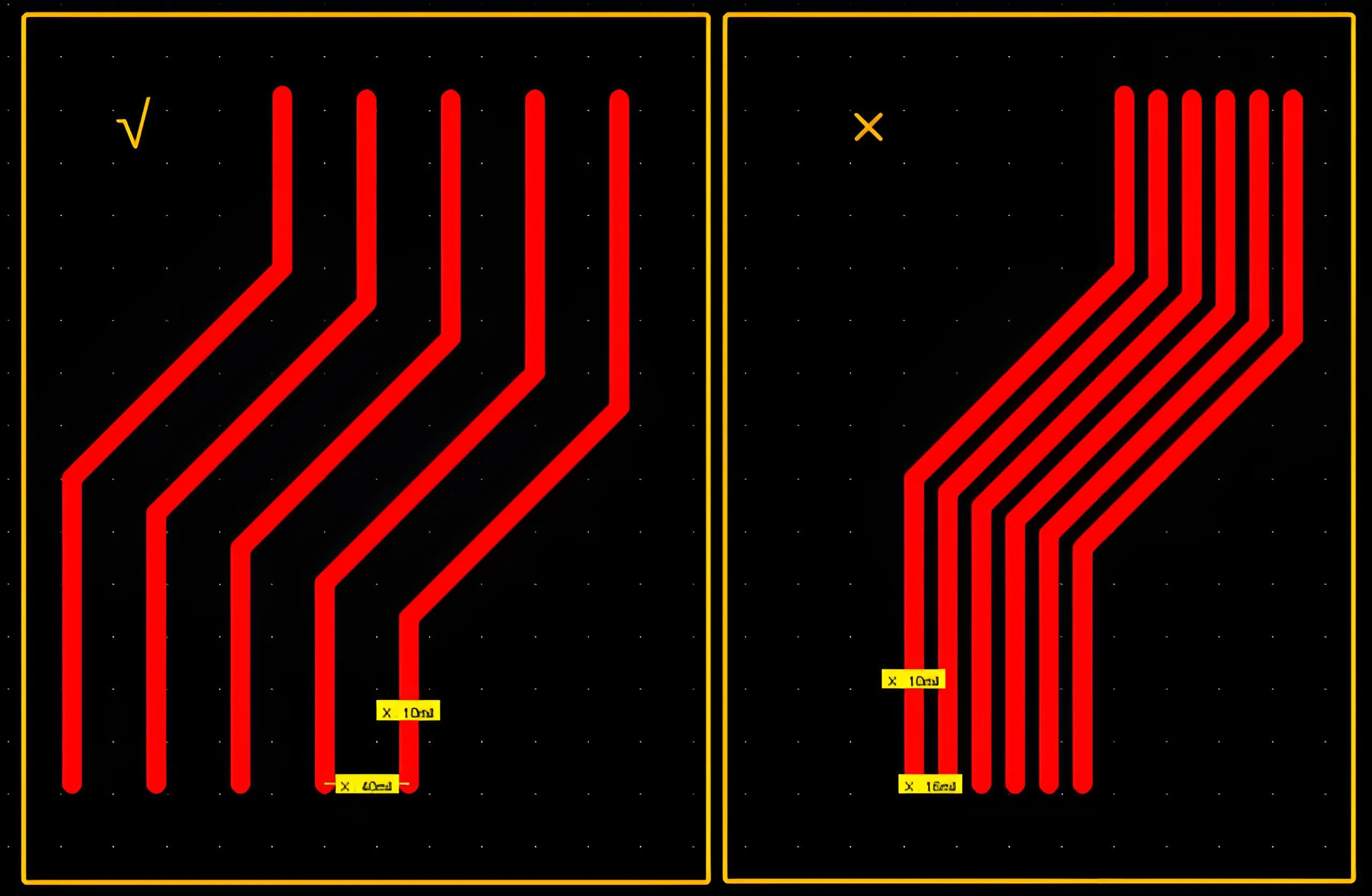
4. Avoid Sharp Corners in Traces
For high-speed signals, avoid 90-degree bends in traces, as they can cause signal reflections. Instead, use 45-degree angles or smooth curves to maintain consistent impedance. This is especially important for traces carrying signals faster than 100 MHz.

Common Mistakes to Avoid with PCB Trace Width in Digital Circuits
Even experienced designers can make mistakes when selecting trace widths for digital circuits. Here are some pitfalls to watch out for.
1. Underestimating Current Needs
Choosing a trace width that's too narrow for the current can lead to overheating and failure. Always double-check current ratings, especially for power lines, and err on the side of wider traces if you're unsure.
2. Ignoring Impedance Matching
For high-speed designs, failing to match trace impedance can result in signal loss or data errors. If your project involves frequencies above 50 MHz, take the time to calculate and verify impedance values for critical traces.
3. Overcomplicating the Layout
While it's tempting to squeeze as many components as possible onto a board, overcrowding can force you to use narrower traces than ideal. Plan your layout carefully to allocate enough space for proper trace widths, especially around high-current or high-speed areas.
Tools and Resources for Selecting PCB Trace Width
Fortunately, there are many tools available to simplify the process of selecting trace widths for digital circuits. Here are a few options that electronic hobbyists and professionals can use.
- Online Calculators: Many websites offer free trace width calculators that factor in current, copper thickness, and temperature rise. These are great for quick estimates.
- Design Software: Most PCB design tools include built-in features for calculating trace width and impedance based on your board's specifications.
- Industry Standards: Refer to guidelines like IPC-2221 for reliable data on trace width versus current capacity. These standards are widely used and provide a solid foundation for any design.
Conclusion: Mastering PCB Trace Width for Digital Circuits
Selecting the right PCB trace width for digital circuits is a fundamental skill for anyone involved in circuit board design. By considering factors like current capacity, signal integrity, and layout constraints, you can ensure that your digital circuits perform reliably and efficiently. Whether you're an electronic hobbyist building a simple project or a seasoned engineer working on high-speed designs, the principles of trace width selection remain the same: plan carefully, use the right tools, and prioritize performance over aesthetics.
With the tips and strategies outlined in this guide, you're well-equipped to tackle the challenges of PCB layout for digital projects. Remember to double-check your calculations, account for manufacturing limitations, and always test your designs to confirm they meet your expectations. A well-designed circuit board trace layout is the foundation of any successful digital circuit, and mastering trace width is a big step toward achieving that goal.


