 ALLPCB


Printed Circuit Board (PCB) design is a complex process where precision and foresight are critical. As electronic devices become smaller, faster, and more intricate, engineers face increasing challenges in ensuring signal integrity, power delivery, and electromagnetic compatibility (EMC). Electromagnetic (EM) simulation tools for pre-layout analysis have emerged as indispensable allies, enabling designers to predict and address potential issues before committing to a physical layout. In this blog, we explore the role of these tools, their key features, and how they empower engineers to create reliable, high-performance PCBs. Whether you're tackling high-speed designs or compact IoT devices, understanding EM simulation can transform your design process.
Why Pre-Layout EM Simulation Matters
Pre-layout analysis occurs early in the PCB design cycle, before components are placed or traces are routed. At this stage, engineers define the schematic, select components, and establish design constraints. EM simulation tools allow designers to model electromagnetic behavior, such as signal propagation, crosstalk, and impedance mismatches, without a physical prototype. This predictive capability is crucial for several reasons:
-
Signal Integrity: High-speed signals, operating at frequencies above 1 GHz, are prone to issues like reflections and crosstalk. Pre-layout simulation helps optimize trace lengths and stack-up configurations to maintain signal integrity.
-
Power Integrity: Voltage drops and noise in the power distribution network (PDN) can degrade performance. EM tools identify areas of high current density, enabling designers to adjust copper weights or add decoupling capacitors.
-
EMC Compliance: Electromagnetic interference (EMI) can lead to regulatory failures. Simulating EMI early ensures compliance with standards like FCC or CISPR.
-
Cost and Time Savings: Identifying issues before layout reduces costly redesigns and accelerates time-to-market.
By addressing these challenges upfront, EM simulation tools provide a foundation for robust PCB designs, especially in applications like 5G, automotive electronics, and medical devices.
Key Features of EM Simulation Tools
Not all EM simulation tools are created equal. The best tools offer a combination of accuracy, usability, and integration with PCB design workflows. Here are the essential features engineers should look for:
1. Accurate Electromagnetic Modeling
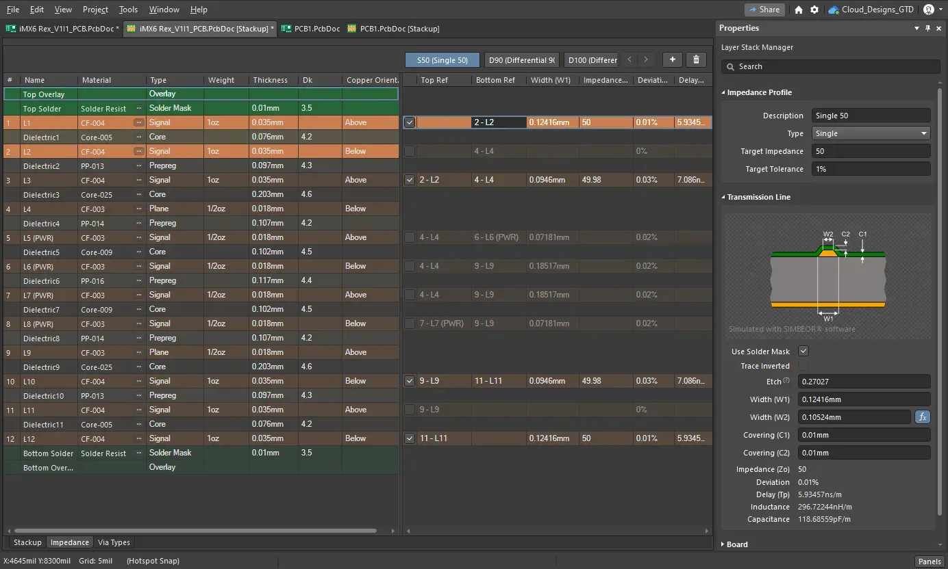
EM simulation tools use computational methods like finite element method (FEM) or method of moments (MoM) to model electromagnetic fields. These models predict how signals behave in complex geometries, such as differential pairs or multilayer stack-ups. For example, a tool might calculate the characteristic impedance of a 50-ohm trace, ensuring it matches the driver and receiver to prevent reflections.
2. Signal and Power Integrity Analysis
Tools like Ansys SIwave or Cadence Sigrity analyze signal integrity by simulating parameters like eye diagrams, jitter, and crosstalk. For power integrity, they assess PDN impedance, targeting values below 1 mΩ at critical frequencies (e.g., 100 MHz) to minimize voltage fluctuations. These analyses help engineers define constraints, such as trace widths of 5 mils for high-speed signals or capacitor placements within 100 mils of IC pins.
3. 3D Field Visualization
Visualizing electromagnetic fields in 3D helps engineers identify hot spots, such as areas of high current density (>10 A/mm²) or EMI radiation. Tools like Keysight ADS or Altium Designer with Ansys integration provide interactive 3D plots, making it easier to pinpoint design flaws.
4. Integration with EDA Software
Seamless integration with electronic design automation (EDA) tools, such as Altium Designer, OrCAD, or KiCad, streamlines the workflow. Engineers can import schematics, apply simulation results to layout constraints, and export optimized designs without manual data translation, reducing errors.
5. Scalability for Complex Designs
High-speed designs with multiple layers (e.g., 12-layer boards) or high-density interconnects (HDI) require scalable solvers. Tools like Mentor Graphics HyperLynx handle large designs efficiently, simulating thousands of nets in minutes, compared to hours for less optimized tools.
Popular EM Simulation Tools for Pre-Layout Analysis
Several EM simulation tools stand out for their capabilities in pre-layout analysis. Below, we review some of the most widely used options, drawing on industry insights and technical specifications.
1. Ansys SIwave
Ansys SIwave is a powerhouse for signal and power integrity analysis. It uses hybrid solvers to model PCB structures, delivering accurate results for impedance, crosstalk, and EMI. For example, SIwave can simulate a differential pair with 100-ohm impedance, identifying mismatches that cause signal degradation. Its EMI Scanner checks for compliance with standards like CISPR 25, flagging potential issues in automotive designs. SIwave integrates with Ansys HFSS for full 3D EM analysis, though it requires significant computational resources.
2. Cadence Sigrity
Cadence Sigrity excels in high-speed design analysis, offering tools for signal integrity, power integrity, and thermal co-simulation. Its PowerSI module analyzes PDN impedance, targeting values below 0.5 mΩ at 1 GHz, while the XtractIM tool extracts parasitic parameters like resistance (R), inductance (L), and capacitance (C). Sigrity's integration with Cadence Allegro ensures a smooth transition from pre-layout to post-layout analysis.
3. Keysight ADS (Advanced Design System)
Keysight ADS is favored for RF and microwave designs, where signal frequencies exceed 10 GHz. Its EM simulation engine, Momentum, models planar structures like microstrip lines, ensuring accurate impedance control (e.g., ±5% tolerance). ADS also supports transient analysis, simulating signal propagation delays as low as 10 ps. Its learning curve is steep, but it's ideal for engineers working on 5G or radar systems.
4. Mentor Graphics HyperLynx
HyperLynx offers a user-friendly interface and fast simulation times, making it accessible to both novice and experienced engineers. It supports DDR4 and PCIe designs, simulating signal rise times as short as 100 ps. HyperLynx's power integrity tools identify voltage drops exceeding 50 mV, guiding capacitor placement. Its integration with Mentor Xpedition enhances collaboration across design teams.
5. Altium Designer with Ansys Integration
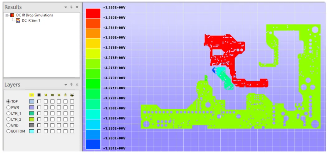
Altium Designer, when paired with Ansys tools like HFSS or SIwave, provides a unified platform for pre-layout simulation. It supports DC power integrity analysis, identifying areas with excessive voltage drops (>100 mV). Altium's PDN Analyzer visualizes power dissipation, helping engineers optimize copper thickness (e.g., 2 oz/ft² for high-current paths). This combination is cost-effective for small to mid-sized teams.
Best Practices for Using EM Simulation Tools
To maximize the benefits of EM simulation, engineers should follow these best practices:
-
Define Clear Design Constraints: Specify impedance targets (e.g., 50 ohms for single-ended signals, 100 ohms for differential pairs) and PDN requirements (e.g., impedance <1 mΩ at 100 MHz) before simulation.
-
Start with Simplified Models: Begin with 2D or quasi-3D models to reduce computation time, then refine with full 3D simulations for critical nets.
-
Validate with Real-World Data: Compare simulation results with measurements from prototypes to calibrate models. For instance, verify simulated crosstalk levels (<–60 dB) against actual board performance.
-
Iterate Early and Often: Use simulation results to adjust stack-up, trace widths, or component placements before finalizing the layout. For example, widen traces from 5 mils to 7 mils to reduce impedance mismatches.
-
Leverage Automation: Use tools with automated design rule checks (DRCs) to flag issues like unconnected pins or spacing violations (<5 mils).
Challenges and Limitations
While EM simulation tools are powerful, they come with challenges:
-
Computational Complexity: Full 3D simulations for large boards (e.g., 16 layers, 5000 nets) can take hours, requiring high-performance workstations.
-
Learning Curve: Tools like Keysight ADS or Ansys SIwave demand expertise in EM theory and software navigation.
-
Model Accuracy: Inaccurate material properties (e.g., dielectric constant of FR-4 varying from 4.2 to 4.7) can skew results.
-
Cost: Licenses for tools like Cadence Sigrity or Ansys SIwave can exceed $10,000 annually, posing barriers for small teams.
To overcome these, engineers can use cloud-based platforms like SimScale for scalable computing or opt for cost-effective tools like KiCad with open-source EM plugins for simpler designs.
How ALLPCB Supports Your PCB Design Journey
For engineers leveraging EM simulation tools, translating optimized designs into high-quality prototypes is the next critical step. ALLPCB's advanced manufacturing capabilities and quick-turn prototyping services streamline this process. With global logistics ensuring delivery in as little as 24 hours, we help you test and validate your designs rapidly. Our state-of-the-art facilities support complex multilayer boards, HDI design, and precise impedance control, aligning perfectly with the requirements identified during pre-layout analysis. By partnering with ALLPCB, you can confidently move from simulation to production, knowing your boards meet the highest standards of quality and reliability.
Conclusion
EM simulation tools for pre-layout analysis are game-changers in PCB design, enabling engineers to predict and resolve issues before they escalate. By modeling signal integrity, power delivery, and EMI, tools like Ansys SIwave, Cadence Sigrity, and Keysight ADS empower designers to create reliable, high-performance boards. Following best practices—such as defining clear constraints and iterating early—maximizes their value, while overcoming challenges like computational complexity ensures accessibility for all teams. As you embark on your next PCB project, consider integrating EM simulation into your workflow to achieve superior results with fewer iterations. With the right tools and a trusted manufacturing partner, your designs can reach their full potential.


