 ALLPCB


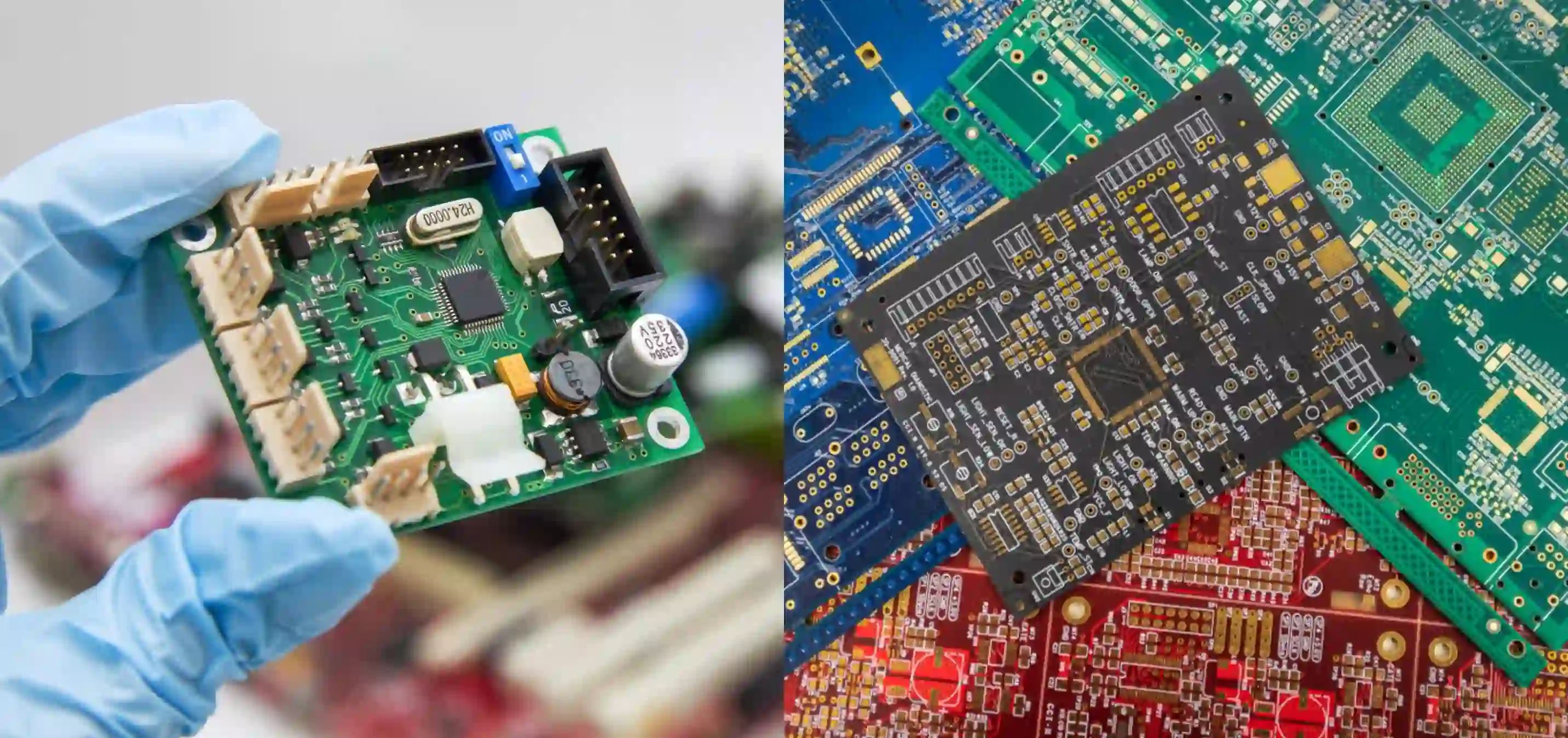
If you're diving into the world of electronics manufacturing, you might be wondering about the difference between a bare board and an assembled PCB, especially in the context of Surface Mount Technology (SMT). Simply put, a bare board is the raw, unpopulated printed circuit board without any components attached, while an assembled PCB is the complete board with all electronic components mounted and soldered in place, ready for use. In SMT, this distinction is critical as it affects every stage of PCB manufacturing, from design to testing. In this blog, we'll explore these differences in detail, focusing on SMT processes, PCB manufacturing stages, component placement, and testing assembly to help you understand each step of the journey.
What Are Bare Boards and Assembled PCBs?
Let's start with the basics. A bare board, also known as a blank PCB, is essentially the foundation of any electronic device. It’s a flat board made of materials like FR-4 (a type of fiberglass epoxy) with conductive copper traces etched onto it to form the circuit layout. At this stage, there are no components—no resistors, capacitors, or chips. It’s just the "skeleton" of the circuit, waiting to be populated.
On the other hand, an assembled PCB is the finished product after components have been mounted and soldered onto the bare board. In the context of SMT, this means tiny components are placed directly onto the surface of the board using automated machines and then soldered through a process called reflow soldering. The assembled PCB is what powers your devices, from smartphones to industrial machinery, once it passes testing.
Understanding these two stages is essential for anyone involved in electronics design or manufacturing, as they represent the starting point and the end goal of the PCB production process.
The Role of Surface Mount Technology (SMT) in PCB Manufacturing
Surface Mount Technology, or SMT, is a method of assembling electronic components directly onto the surface of a PCB. Unlike older through-hole technology, where component leads are inserted into drilled holes, SMT components are smaller and sit flat on the board. This allows for higher component density, faster assembly, and more compact designs, which are critical for modern electronics like laptops and wearables.
In SMT, the journey from a bare board to an assembled PCB involves several precise stages. Each step is designed to ensure accuracy and reliability, as even a small error can lead to a malfunctioning board. Let’s break down these stages to see how bare boards transform into fully assembled PCBs.
PCB Manufacturing Stages: From Bare Board to Assembled PCB in SMT
The process of turning a bare board into an assembled PCB using SMT involves multiple stages. Each stage builds on the last, ensuring that the final product meets design specifications and quality standards. Below are the key PCB manufacturing stages in SMT:
1. Design and Fabrication of the Bare Board
Everything starts with the design of the PCB layout using specialized software. Engineers create a digital blueprint that defines where copper traces, pads, and vias will be placed. Once the design is finalized, the bare board is fabricated. This involves layering insulating material with copper, etching away excess copper to form traces, and drilling holes for vias or mounting points. At the end of this stage, you have a bare board with no components—just the conductive pathways ready for assembly.
Key Fact: The typical thickness of copper on a bare board ranges from 1 oz (35 micrometers) to 2 oz (70 micrometers) per square foot, depending on the current-carrying requirements of the circuit.
2. Solder Paste Application
Once the bare board is ready, the SMT assembly process begins with applying solder paste to specific areas where components will be placed. Solder paste, a mixture of tiny solder particles and flux, is applied using a stencil—a thin metal sheet with cutouts matching the component pads on the board. This ensures that paste is only applied to the exact spots needed for soldering.
This step is critical because uneven or excessive solder paste can lead to issues like solder bridging, where adjacent pads connect unintentionally, causing short circuits.
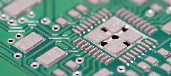
3. Component Placement in SMT
With solder paste in place, the next stage is component placement. In SMT, this is typically done using automated pick-and-place machines. These machines are incredibly fast and precise, capable of placing over 100,000 components per hour on some high-end models. They pick up tiny components like resistors, capacitors, and integrated circuits (ICs) from reels or trays and position them onto the solder paste-covered pads of the bare board.
The precision of component placement in SMT is vital. For example, modern components like 0201 resistors (measuring just 0.6 mm x 0.3 mm) require placement accuracy within 0.1 mm to ensure proper soldering and functionality. Misalignment at this stage can lead to poor connections or complete failure of the board.
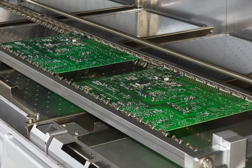
4. Reflow Soldering
After components are placed, the board goes through a reflow oven. This is where the solder paste melts and forms a permanent bond between the components and the board. The oven heats the board in stages—preheating, soaking, reflow, and cooling—to ensure even melting and to prevent thermal shock to components. Peak temperatures in the reflow zone often reach around 240–260°C for lead-free solder, which is common in SMT due to environmental regulations.
At the end of this stage, the bare board has officially transformed into an assembled PCB, with all components securely soldered in place.
5. Inspection and PCB Testing Assembly
Once soldering is complete, the assembled PCB undergoes rigorous inspection and testing to ensure it functions as intended. This is a critical difference between a bare board and an assembled PCB—testing only happens after assembly, as bare boards have no components to test.
Common inspection methods in SMT include Automated Optical Inspection (AOI), which uses cameras to detect misaligned components or solder defects. AOI systems can scan a board in seconds, identifying issues like missing components or solder bridging with over 95% accuracy on advanced setups. For more complex boards, X-ray inspection may be used to check hidden solder joints under components like Ball Grid Arrays (BGAs).
After inspection, functional testing or in-circuit testing (ICT) is performed. ICT uses probes to check electrical connections and component values, ensuring the assembled PCB meets design specifications. For instance, ICT can measure resistance values to confirm a resistor is within its specified range, such as 1 kΩ ±5%.
Key Differences Between Bare Board and Assembled PCB in SMT
Now that we’ve covered the manufacturing stages, let’s summarize the key differences between a bare board and an assembled PCB, specifically in the context of SMT:
- Components: A bare board has no components; it’s just the raw PCB with copper traces. An assembled PCB has all SMT components mounted and soldered in place.
- Functionality: A bare board cannot function as it lacks electronic parts. An assembled PCB is a working circuit ready for integration into a device, pending successful testing.
- Manufacturing Stage: Bare boards are the output of the fabrication stage, while assembled PCBs are the result of SMT assembly processes like component placement and reflow soldering.
- Testing: Bare boards may undergo basic checks for trace continuity or shorts, but comprehensive testing like ICT or functional testing only applies to assembled PCBs.
- Cost: Bare boards are significantly cheaper since they involve only fabrication. Assembled PCBs cost more due to the added expense of components, labor, and SMT assembly processes.
Why Understanding This Difference Matters
For engineers, designers, and manufacturers, knowing the distinction between bare boards and assembled PCBs in SMT is crucial for several reasons. First, it helps in planning the production timeline and budget. Fabrication of bare boards might take a few days, while SMT assembly can add another few days or weeks depending on complexity and volume.
Second, it impacts troubleshooting. If a design flaw is found in the bare board stage, it’s much cheaper to revise and re-fabricate before assembly. Once components are soldered, rework becomes costly and time-consuming. For example, removing and replacing a single BGA component on an assembled PCB can cost upwards of $50 per part due to specialized equipment and labor.
Lastly, this knowledge aids in communication with manufacturing partners. Specifying whether you need just bare boards or fully assembled PCBs ensures clarity and prevents delays in the production process.
Challenges in SMT Assembly: Bare Board to Assembled PCB
Transitioning from a bare board to an assembled PCB in SMT isn’t always straightforward. Challenges can arise at various stages:
- Design Errors: If the bare board layout has errors, such as incorrect pad sizes for SMT components (e.g., pads too small for a 0402 capacitor), it can lead to poor soldering or component misalignment during assembly.
- Component Placement Issues: High-density designs in SMT can result in placement errors if the pick-and-place machine isn’t calibrated correctly, leading to yields as low as 80% in extreme cases.
- Soldering Defects: Issues like tombstoning (where one end of a component lifts off the pad) or cold solder joints can occur during reflow, requiring rework on the assembled PCB.
- Testing Failures: Even after assembly, some PCBs fail functional testing due to undetected defects, necessitating costly repairs or redesigns.
Addressing these challenges requires careful design validation, quality control during SMT assembly, and thorough PCB testing assembly protocols.
Conclusion: Navigating the Journey from Bare Board to Assembled PCB in SMT
The difference between a bare board and an assembled PCB is night and day in the world of SMT. A bare board is the starting point—a raw canvas of copper traces waiting to be brought to life. An assembled PCB, on the other hand, is the finished masterpiece, complete with components placed and soldered via SMT processes, ready to power your electronic devices after rigorous testing.
By understanding the PCB manufacturing stages, from design and fabrication to component placement in SMT and PCB testing assembly, you can better manage your projects, avoid costly mistakes, and ensure high-quality results. Whether you’re an engineer designing a new circuit or a manufacturer overseeing production, this knowledge is your foundation for success in electronics manufacturing.
At ALLPCB, we’re committed to supporting you through every step of this process, ensuring that your transition from bare board to assembled PCB is seamless and efficient. Let’s build the future of electronics together with precision and innovation.


