 ALLPCB


Introduction
High-speed PCB HDI design has become essential for modern electronics that demand compact form factors and superior performance. As devices operate at frequencies exceeding several gigahertz, engineers face intensified pressure to pack more functionality into smaller spaces while preserving signal integrity. High Density Interconnect (HDI) technology addresses these needs through advanced via structures and finer routing features. However, achieving high routing density introduces challenges like crosstalk, impedance discontinuities, and increased layer count. This article explores strategies to overcome these density challenges in high-speed applications. By focusing on microvias, blind vias, buried vias, and optimized stackups, designers can balance miniaturization with reliable operation.
HDI PCBs enable high-speed signals to traverse dense layouts without excessive degradation. Engineers must consider via transitions, trace spacing, and material properties from the outset. Proper implementation reduces signal loss and electromagnetic interference. Ultimately, mastering these elements ensures compliance with performance requirements in telecommunications, computing, and automotive systems.
Understanding HDI PCBs and Their Relevance to High-Speed Applications
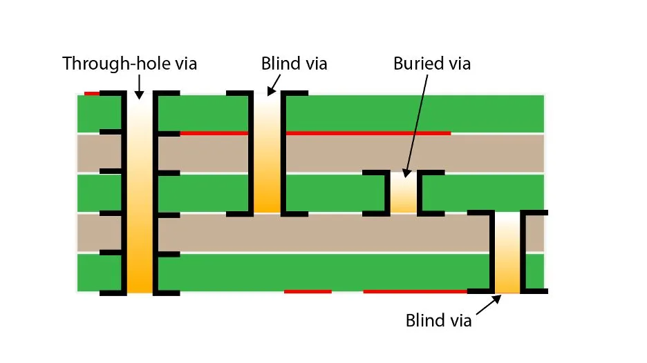
HDI PCBs represent an evolution in printed circuit board technology, characterized by finer features and higher interconnection density compared to standard multilayer boards. They incorporate microvias, which are laser-drilled vias typically smaller than 150 micrometers in diameter, as defined in industry guidelines. Blind vias connect outer layers to inner layers without penetrating the full board thickness, while buried vias interconnect internal layers exclusively. These structures allow for greater routing density and reduced layer count in high-speed designs.
In high-speed applications, HDI technology matters because signal rise times shorten dramatically, amplifying sensitivity to reflections and noise. Miniaturization drives the need for finer pitch components, such as ball grid arrays with 0.4 mm or smaller spacing, which standard PCBs struggle to support. HDI enables shorter signal paths, minimizing propagation delays and attenuation. According to IPC-2226A, HDI constructions are classified into types like Type I, II, and III based on microvia layering, guiding designers toward appropriate build-ups for specific density needs.
The relevance extends to layer count optimization, where HDI reduces overall thickness while supporting complex routing. For instance, staggered microvias prevent alignment issues that could compromise yield. High-speed PCB HDI design thus facilitates integration of high pin-count devices without sacrificing electrical performance.
Key Technical Principles in High-Speed HDI Design
The foundation of high-speed PCB HDI design lies in via technologies that enhance routing density without introducing excessive parasitics. Microvias provide vertical interconnects with minimal stub length, crucial for maintaining signal integrity at multi-gigabit speeds. Blind vias eliminate unnecessary through-hole penetrations, freeing surface area for traces and components. Buried vias further optimize inner layer space, allowing dense power and ground planes adjacent to signal layers.
Signal integrity principles dictate careful management of impedance and crosstalk. In dense HDI layouts, trace widths narrow to 50 micrometers or less, paired with equivalent spaces to control characteristic impedance around 50 or 100 ohms for single-ended or differential pairs. Length matching ensures skew below acceptable limits, typically a fraction of the signal rise time. Vias act as discontinuities, so their placement and fanout from fine-pitch BGAs require precise planning to avoid resonance.
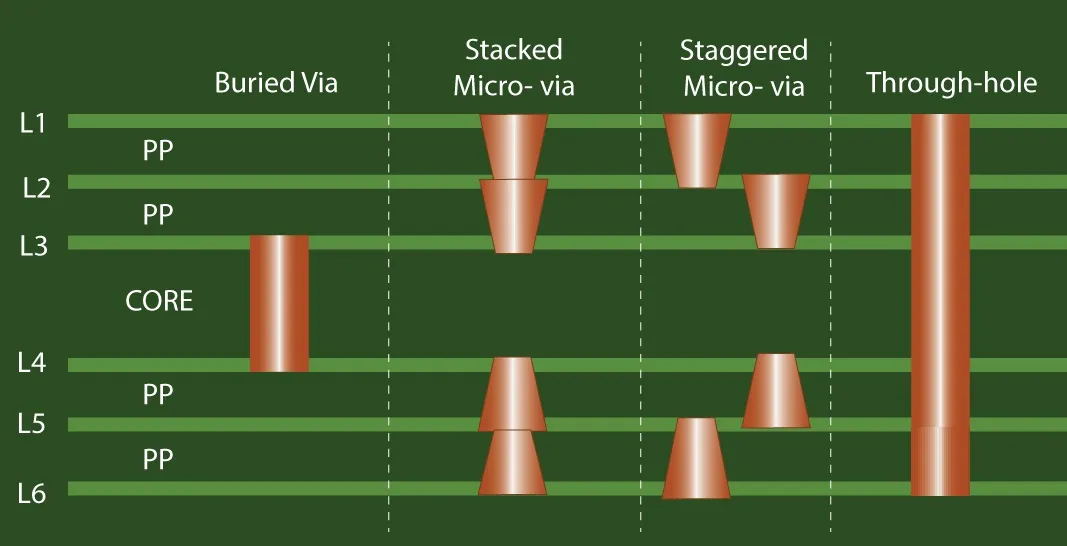
Layer stackup configuration influences these principles profoundly. Core and prepreg selection affects dielectric constants, impacting propagation velocity. Sequential lamination builds HDI layers incrementally, enabling stacked or staggered microvia configurations. IPC-2226A outlines aspect ratios and drill sizes to ensure reliable plating and reliability under thermal stress.
Thermal management integrates into these principles, as dense routing elevates heat density. Vias serve as thermal conduits, but excessive density risks hotspots. Engineers balance via fields with plane cutouts strategically.
Related Reading: HDI PCB Stackup: Mastering Layer Configuration for Optimal Performance
Primary Challenges: Routing Density, Signal Integrity, and Layer Count
High routing density in HDI PCBs challenges designers with congestion around high I/O components. Fine-pitch devices demand escape routing through multiple via layers, complicating trace allocation. Microvias and blind vias alleviate this by providing direct inner layer access, yet misalignment during lamination can create opens or shorts. Buried vias help, but their placement requires foresight to avoid blocking future routes.
Signal integrity issues escalate with density. Crosstalk arises from capacitive and inductive coupling between closely spaced traces, degrading eye diagrams. Impedance mismatches at via transitions cause ringing, particularly in high-speed signals with fast edges. Reflections from unterminated stubs in through vias exacerbate this, necessitating blind and buried alternatives.
Layer count optimization poses another hurdle in high-speed PCB HDI design. Adding layers increases cost and thickness, but insufficient layers lead to suboptimal routing. Miniaturization goals conflict with signal separation needs for integrity. IPC-6016D specifies performance criteria that HDI must meet, including thermal cycle endurance for microvias.
Manufacturing tolerances amplify these challenges. Laser drilling precision for microvias must hold within microns, and plating uniformity prevents voids. Designers contend with yield trade-offs when pushing density limits.
Related Reading: Unlocking Density: A Deep Dive into High-Density Interconnect (HDI) Multilayer PCBs
Practical Solutions and Best Practices
Engineers overcome routing density challenges through systematic stackup planning and via optimization. Begin with HDI Type selection: Type II for moderate density with one build-up on each side, escalating to Type III for complex needs. Staggered microvias reduce stress concentrations compared to stacked, improving reliability while maintaining density. Allocate via budgets per net class, prioritizing high-speed signals for shortest paths.
For signal integrity, implement controlled impedance traces with consistent widths and spaces. Use differential routing for clocks and data lines, ensuring pair symmetry. Via optimization includes back-drilling if through vias persist, or teardrop pads to ease current crowding. Simulation verifies pre-layout integrity, modeling via stubs and crosstalk.
Layer count minimization relies on efficient partitioning. Group high-speed signals between ground planes for shielding. Microvias enable any-layer interconnects in advanced HDI, slashing layer needs by 20 to 30 percent in dense designs. Balance power distribution with buried vias feeding plane splits.
Best practices include design rule checks tailored to HDI, enforcing minimum annular rings and clearances. Collaborate early with fabrication capabilities for via sizes and aspect ratios. Thermal vias under hotspots, combined with copper balancing, mitigate warpage.
Material selection supports these practices, favoring low-loss dielectrics for high frequencies. Sequential build-up processes align layers precisely, crucial for blind via registration.
Testability integrates via-in-pad for probes, enhancing debug in dense boards.
Conclusion
High-speed PCB HDI design triumphs over density challenges through strategic use of microvias, blind vias, buried vias, and disciplined stackup engineering. Routing density improves with via optimization, while signal integrity holds via impedance control and short paths. Layer count reductions via HDI enable true miniaturization without performance loss. Adhering to guidelines like IPC-2226A ensures robust outcomes. Engineers equipped with these principles deliver reliable boards for demanding applications. Future advancements will further refine these techniques, pushing density boundaries.
FAQs
Q1: What role do microvias play in high-speed PCB HDI design?
A1: Microvias enable high routing density by providing compact vertical connections with low parasitics, ideal for fine-pitch components. In high-speed applications, their small size minimizes stub inductance, preserving signal integrity. IPC-2226A defines them as under 150 micrometers, supporting stacked or staggered configurations. Designers use them to escape BGAs efficiently, reducing layer count needs.
Q2: How do blind vias and buried vias improve signal integrity in HDI boards?
A2: Blind vias connect surface to inner layers without full penetration, shortening return paths and cutting crosstalk. Buried vias optimize inner routing, allowing ground planes near signals for better shielding. Together, they enhance impedance control in dense layouts. This setup is critical for high-speed signals, minimizing discontinuities.
Q3: What are common strategies for managing routing density in high-speed HDI design?
A3: Prioritize via staggering to boost density without reliability risks. Partition signals by speed, using microvias for critical nets. Optimize stackups to minimize layers while ensuring plane proximity. Early DRCs and simulations prevent congestion.
Q4: How does HDI facilitate miniaturization while addressing layer count concerns?
A4: HDI uses advanced vias to interconnect densely, reducing overall board thickness and layers compared to conventional multilayers. Microvias and any-layer via concepts support fine features for compact devices. This balances high-speed performance with size constraints effectively.


