 ALLPCB


Introduction
Vias serve as critical interconnects in multilayer printed circuit boards, enabling signal routing between layers while maintaining compact designs. However, during reflow soldering in assembly, solder can wick into untented or unplugged vias through capillary action, leading to insufficient solder fillets on component pads and compromised joint integrity. This phenomenon, known as solder wicking, reduces mechanical strength and electrical reliability, particularly in high-density interconnects. The via tenting process and via plugging process address these issues by providing protective barriers that block solder ingress and enhance overall board performance. Reliability via tenting and plugging becomes essential for applications demanding high yields and long-term durability, such as consumer electronics and automotive systems. By selecting the appropriate method, engineers can mitigate risks associated with solder wicking prevention while balancing fabrication complexity.
What Is Via Tenting and Why Does It Matter?
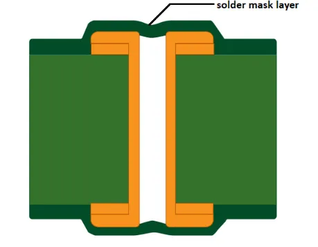
Via tenting involves applying a solder mask layer that spans across the via opening, creating a protective "tent" over the plated through-hole. This process typically uses liquid photoimageable (LPI) solder mask, which offers superior resolution for fine features compared to dry film solder mask (DFSM). The tent seals the via from environmental contaminants like solder paste, flux residues, and moisture during assembly and operation. In the via tenting process, the mask is exposed, developed, and cured to form a taut membrane that withstands reflow temperatures without rupturing in properly designed boards. This method proves vital for non-critical signal vias near component pads, where solder wicking prevention directly impacts assembly yields.
Engineers prioritize via tenting for its simplicity and effectiveness in standard multilayer boards. According to IPC-4761, tented vias fall under Type I categories, such as Type I-a for one-sided tenting or Type I-b for both sides, defining acceptable coverage and inspection criteria. These guidelines ensure consistent protection across production runs. Without tenting, exposed vias invite solder flow during wave or reflow soldering, depleting pad solder volume and risking open joints. Thus, reliability via tenting supports higher class 2 and class 3 assemblies by minimizing defects observable under IPC-A-600 acceptability standards.
The Via Plugging Process Explained
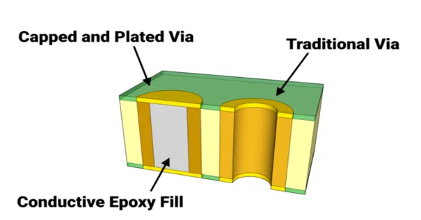
Via plugging takes protection further by filling the via barrel with a material before applying solder mask coverage. Non-conductive epoxy resins or conductive pastes serve as fillers, dispensed via screen printing, inkjet, or vacuum assist methods to achieve complete or partial fill. The via plugging process includes plating the hole, filling, curing the material, and then overcoating with solder mask for a planar surface. This approach suits via-in-pad designs, where components or traces route directly over the via, eliminating air gaps that could trap contaminants. Filled vias exhibit superior thermal conductivity in conductive variants, aiding heat dissipation in power applications.
IPC-4761 classifies plugged vias as Type VI, distinguishing between filled-and-covered configurations that meet stringent planarization requirements. Engineers specify plugging when tenting alone fails for larger diameters or high-reliability needs. The process demands precise control to avoid voids, which could compromise barrel integrity during thermal cycling. Overall, via plugging enhances mechanical stability by distributing stresses evenly across the board structure.
Technical Mechanisms Behind Solder Wicking and Prevention Strategies
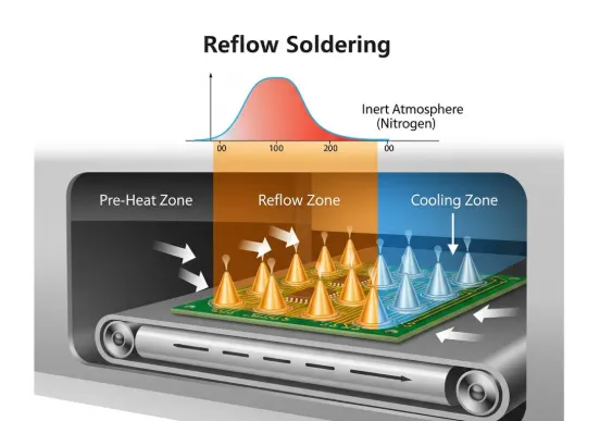
Solder wicking occurs when molten solder encounters an open via during reflow, drawn in by surface tension and wetting along the plated walls. This depletes the solder joint volume on adjacent pads, often resulting in head-in-pillow defects or insufficient standoff. Factors like via diameter, aspect ratio, and reflow profile exacerbate the issue, with larger vias (>0.3 mm) posing greater risks due to increased capillary forces. Tenting interrupts this flow by presenting a non-wettable barrier, while plugging eliminates the void entirely, preventing any ingress.
Reliability via tenting relies on the solder mask's adhesion and tensile strength to maintain integrity through multiple thermal excursions. IPC-6012 outlines performance qualifications, including thermal shock and cross-section analysis to verify tent holdover. Plugging adds robustness against vibration and flexing, as the filler material bonds to the plating, reducing delamination risks. Both methods improve impedance control by stabilizing the via environment, crucial for high-speed signals.
Practical Solutions and Best Practices for Implementation
Designers should limit tenting to vias under 0.3 mm diameter with adequate annular ring widths, typically 0.15 mm minimum, to ensure tent bridging without pinholes. Fabrication notes must specify LPI mask thickness (around 15-25 microns) and tenting sides, aligning with IPC-4761 requirements. For plugging, select non-conductive fill for signal integrity preservation, targeting 100% fill verified by automated X-ray inspection. Process controls include pre-bake to remove moisture and post-cure for filler stability.
Solder wicking prevention extends to stencil design, where smaller apertures over via-in-pad reduce paste volume. Engineers balance via density with panel utilization during quoting, as the cost of via tenting remains minimal as a standard mask process add-on. Via plugging incurs higher costs due to additional material handling and inspection steps, often 20-50% more depending on volume, though it enables denser layouts. Always validate prototypes with cross-sections to confirm compliance.
Comparing Via Tenting and Via Plugging: When to Choose Each
Via tenting suits cost-sensitive designs with peripheral non-signal vias, offering quick implementation without fill materials. It prevents solder wicking effectively for fine-pitch BGAs but may fail under mechanical stress if the tent tears. Plugging excels in HDI boards or BGA fanout, providing a routable surface and full environmental seal. Conductive plugging supports current carrying but risks CTE mismatch-induced cracks.
- Process Complexity — Via Tenting: Low (mask only); Via Plugging: High (fill + mask)
- Via Size Suitability — Via Tenting: <0.3 mm; Via Plugging: Any, especially >0.3 mm or via-in-pad
- Cost Impact — Via Tenting: Minimal; Via Plugging: Moderate to high
- Reliability Gain — Via Tenting: Good for assembly; Via Plugging: Excellent for operation
Troubleshooting Common Issues in Via Protection
Tent tears often stem from excessive via-to-mask clearance or mask overexposure, inspectable via dye-and-peel testing. Voids in plugged vias arise from air entrapment during dispense; vacuum plugging mitigates this. Reliability via tenting falters in high-layer-count boards if drill smear persists, necessitating plasma desmear. Monitor reflow profiles to avoid tent softening above 200°C.
Conclusion
Via tenting and plugging stand as proven strategies for solder wicking prevention, directly boosting PCB reliability through targeted protection. The via tenting process offers economical assembly safeguards, while the via plugging process delivers comprehensive structural enhancements for advanced designs. Engineers must weigh the cost of via tenting against performance needs, guided by IPC standards for optimal outcomes. Implementing these techniques ensures robust interconnects, higher yields, and extended service life in demanding environments.
FAQs
Q1: What is the via tenting process in PCB manufacturing?
A1: The via tenting process applies solder mask over via openings to form a protective bridge, typically using LPI material for high resolution. It seals the plated hole from solder paste and flux during assembly. This method aligns with IPC-4761 Type I definitions, suitable for small vias under 0.3 mm. Tenting enhances reliability by preventing contamination without adding fill steps.
Q2: How does via tenting contribute to solder wicking prevention?
A2: Via tenting blocks molten solder from entering the via barrel via capillary action in reflow soldering. The mask tent maintains integrity under thermal stress, preserving pad solder volume for strong joints. Reliability via tenting reduces defects like insufficient fillets, critical for class 3 boards. It proves cost-effective compared to alternatives for standard applications.
Q3: What are the key differences between the via tenting process and via plugging process?
A3: Tenting covers the via opening with solder mask alone, leaving the barrel open underneath, ideal for simple protection. Plugging fills the via with epoxy before masking, enabling via-in-pad use and full planarization per IPC-4761 Type VI. Tenting costs less but suits smaller vias; plugging offers superior mechanical reliability at higher expense.
Q4: What factors influence the cost of via tenting in PCB production?
A4: The cost of via tenting remains low as it integrates into standard solder mask application, adding minimal time. Larger via arrays or both-sided tenting slightly increase exposure steps. Compared to via plugging, it avoids filler materials and extra inspections. Specify clearly in fab notes to optimize yields and keep costs down.
References
IPC-4761 — Design Guide for Protection of Printed Board Via Structures. IPC, 2006
IPC-6012F — Qualification and Performance Specification for Rigid Printed Boards. IPC, 2023
IPC-A-600M — Acceptability of Printed Boards. IPC, 2025


