 ALLPCB


Introduction
In modern high-speed PCB designs, maintaining signal integrity poses significant challenges for electric engineers. Differential pairs, commonly used in interfaces like LVDS, PCIe, and Ethernet, transmit complementary signals across two closely coupled traces. Length matching ensures these signals arrive at the receiver simultaneously, preventing timing errors that degrade performance. This article explores advanced routing techniques focused on differential pair routing length matching, including serpentine routing PCB design methods and delay tuning for differential signals. Engineers must prioritize these practices to meet stringent high-speed differential routing rules and achieve reliable operation. Understanding these concepts allows designers to minimize intra-pair skew effectively.
What Are Differential Pairs and Why Length Matching Matters
Differential pairs consist of two traces carrying opposite polarity signals, where the receiver detects the voltage difference to reject common-mode noise. This configuration excels in noisy environments but requires precise length matching to avoid skew, the time delay between the pair's signals. Even small length discrepancies, on the order of fractions of the signal's rise time, can convert differential signals into common-mode noise, opening the eye diagram and increasing bit error rates. In high-speed applications exceeding 1 Gbps, differential pair routing length matching becomes critical to preserve signal quality over long traces. Without proper matching, reflections and crosstalk amplify, violating high-speed differential routing rules. Adhering to guidelines from IPC-2221C ensures robust designs that support data rates up to tens of Gbps.
Length mismatches arise from routing constraints, such as detours around components or vias, leading to propagation delay variations. The effective dielectric constant of the PCB material influences signal velocity, making consistent routing paths essential. Minimizing skew differential pairs directly impacts jitter budgets in serial links. Engineers evaluate total trace length from driver to receiver, including vias and bends, to quantify potential skew. Industry practices emphasize tolerances like 5 mils or less for signals above 5 Gbps, though exact values depend on stackup and frequency.
Technical Principles Behind Length Matching
Signal propagation in PCB traces behaves as a transmission line when trace lengths exceed the critical length, defined in IPC-2251 as approximately one-sixth of the signal wavelength. At high frequencies, the phase velocity difference due to unequal lengths introduces skew, quantified as skew = (length difference) * (velocity factor). Velocity factor accounts for the dielectric's effective permittivity, typically 0.6 to 0.7 in FR-4 materials. For a 10 Gbps signal with 100 ps rise time, a 1 mil length mismatch equates to about 6 ps skew, consuming a significant portion of the timing margin. Delay tuning differential signals compensates for these discrepancies by adding intentional detours while preserving impedance.
Impedance control complements length matching, as differential pairs target 90 to 120 ohms characteristic impedance. Variations in trace width, spacing, or layer transitions disrupt this, exacerbating skew effects. Coupled microstrip or stripline configurations influence coupling factors, where tight coupling reduces radiation but demands symmetric routing. Engineers model these using field solvers to predict intra-pair skew before fabrication. Serpentine routing PCB design introduces controlled bends to equalize lengths without excessive radiation.
Layer stacking affects propagation; routing both traces on the same layer simplifies matching but may limit density. Vias introduce stubs that add delay, requiring back-drilling or blind vias for mitigation. Temperature and manufacturing tolerances further influence effective lengths, underscoring the need for design margins.
Key Techniques for Length Matching in Differential Pairs
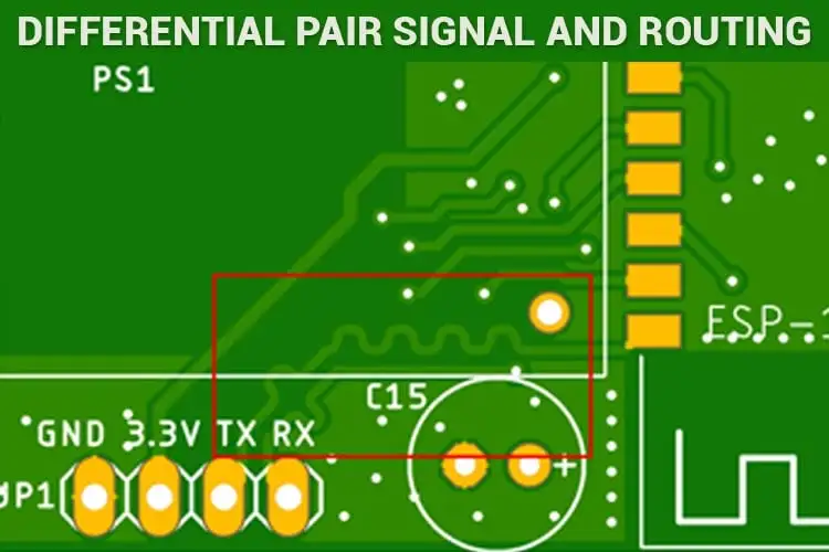
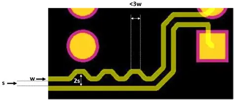
Serpentine routing stands out as a primary method in serpentine routing PCB design, featuring multiple parallel bends to add length incrementally. This technique allows fine adjustments in 1 mil steps by varying bend amplitude and period, ideal for dense boards. Engineers position serpentine sections away from other signals to minimize crosstalk, ensuring bends maintain constant spacing. Amplitude should not exceed five times the trace width to avoid resonance at high frequencies. This approach excels in delay tuning differential signals for USB 3.0 or DDR interfaces.
Trombone or accordion routing offers another option, resembling a folded pattern that folds back on itself for length equalization. It provides larger adjustments but consumes more space and risks coupling to adjacent folds. For minimal area impact, engineers prefer straight-line extensions with 45-degree miters over sharp 90-degree corners, which cause reflections. High-speed differential routing rules dictate smooth transitions to preserve signal fidelity.
Delay tuning involves interactive tools that automatically generate matching structures, verifying against skew budgets. Manual verification confirms total length parity within tolerances. Combining techniques, such as serpentine followed by trombone, handles complex topologies like fanouts from BGA packages.
High-Speed Differential Routing Rules for Minimizing Skew
High-speed differential routing rules prioritize symmetry: maintain constant edge-coupled spacing, typically 4 to 8 mils between traces, and 3H spacing to adjacent signals, where H is trace height above reference plane. Route pairs parallel over continuous reference planes to avoid slotting-induced skew. Avoid splitting planes under pairs, as this creates impedance discontinuities. Per IPC-2141A, calculate controlled impedance early in stackup planning to support length matching.
Minimize vias by routing on outer layers when possible, and use via-in-pad for density. For layer changes, employ broadside coupled vias with symmetric fanouts. Length tuning tolerances tighten with frequency: under 0.1% of total length for 25 Gbps signals. Pre-emphasis at drivers compensates minor skew but cannot replace routing precision.
Crosstalk mitigation involves orthogonal routing for perpendicular layers and shielding with ground traces. Simulate post-layout to validate eye height and jitter, iterating on length matching as needed.
Best Practices and Troubleshooting Common Issues
Start with schematic constraints defining pair nets and max skew, propagating to layout. Use length-matching modes during interactive routing, tuning one trace while locking the other. Verify post-route with reports comparing + and - net lengths. Common pitfalls include over-tuning causing loops that radiate EMI or manufacturing defects from tight bends.
In troubleshooting, excessive skew manifests as intermittent data errors or eye closure in simulations. Inspect for asymmetric vias or plane voids. For multilayer boards, account for different propagation delays between microstrip and stripline. Always incorporate design rule checks for high-speed differential routing rules.
Field testing with TDR confirms impedance and delay uniformity. Collaborate with fabricators early on capabilities like resolution for serpentine features.
Conclusion
Mastering differential pair routing length matching elevates PCB performance in high-speed applications. Techniques like serpentine routing PCB design and delay tuning differential signals, guided by high-speed differential routing rules, effectively minimize skew differential pairs. Logical application of these methods, aligned with standards like IPC-2221C, IPC-2141A, and IPC-2251, ensures signal integrity. Engineers benefit from structured workflows that integrate simulation and verification. Prioritizing these advanced routing techniques yields reliable, low-jitter designs ready for demanding environments.
FAQs
Q1: What is the importance of differential pair routing length matching in high-speed designs?
A1: Differential pair routing length matching ensures signals in the pair propagate with equal delay, minimizing intra-pair skew that distorts eye patterns. For data rates above 5 Gbps, mismatches exceed timing budgets, causing errors. Techniques like serpentine routing PCB design adjust lengths precisely while maintaining impedance. Engineers follow high-speed differential routing rules to keep tolerances under 10 mils typically.
Q2: How does serpentine routing PCB design help in delay tuning differential signals?
A2: Serpentine routing introduces controlled wiggles to equalize trace lengths without altering overall path direction. It allows granular adjustments by varying bend count and amplitude, suitable for dense layouts. Maintain pair spacing constant to preserve coupling. This method minimizes skew differential pairs effectively in protocols like PCIe.
Q3: What are key high-speed differential routing rules for minimizing skew differential pairs?
A3: Maintain symmetric spacing, route over solid planes, and limit length mismatch to rise time fractions. Avoid vias under pairs and use 45-degree bends. Per IPC-2141A, verify impedance targets early. Post-layout simulation confirms compliance.
Q4: When should engineers apply length matching to differential pairs?
A4: Apply when trace lengths exceed critical length per IPC-2251, or for signals over 1 GHz. Always for SerDes links to meet jitter specs. Use tools for automatic tuning during routing.
References
IPC-2221C — Generic Standard on Printed Board Design. IPC, 2023
IPC-2141A — Design Guide for High-Speed Controlled Impedance Circuit Boards. IPC, 2004
IPC-2251 — Design Guide for the Packaging of High-Speed Electronic Circuits. IPC


