ALLPCB


Introduction
PCB panelization combines multiple individual circuit boards into a single larger panel to streamline manufacturing processes, from fabrication to assembly. This approach reduces handling time, minimizes setup costs per board, and improves throughput in high-volume production. However, the shape of the PCB fundamentally influences panelization strategies, as rectangular boards align seamlessly with standard methods while complex contours demand specialized techniques. Engineers must consider PCB shape panelization early in design to balance material efficiency, depaneling reliability, and overall yield.
Rectangular PCB panelization typically leverages straightforward scoring or routing, allowing tight packing and predictable separation. In contrast, panelizing irregular PCBs introduces challenges like increased scrap material and mechanical stress during depaneling. Optimizing space for complex shapes requires careful layout planning, often aided by CAD software panelization tools. These differences not only affect cost but also impact quality control, as irregular edges can lead to variations in tolerances and handling.
Understanding these dynamics empowers electrical engineers to make informed decisions that align with production capabilities. Factory insights reveal that poor shape consideration can result in up to significant waste or rework, underscoring the need for strategic panel design. This article explores the technical principles, best practices, and comparative strategies to guide optimal PCB shape panelization.
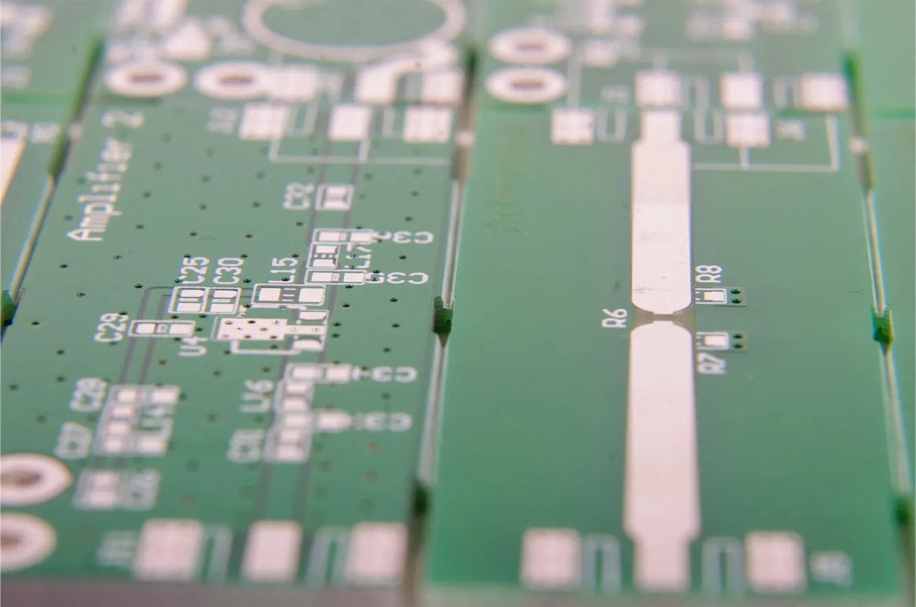
What Is PCB Panelization and Why Does Shape Matter?
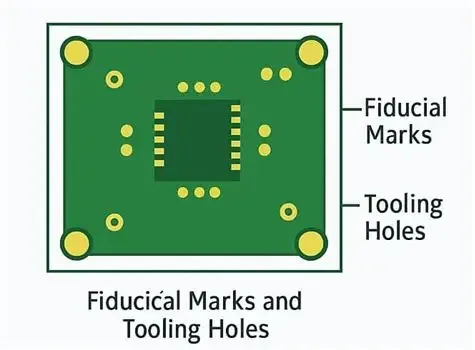
PCB panelization involves arraying multiple boards on a production panel, typically rectangular, to process them simultaneously through etching, drilling, plating, and assembly steps. Common methods include V-scoring for linear separation, tab routing for flexible holding points, and full routing for intricate detachment. The panel frame, or rails, provides stability during automated handling, with fiducials ensuring precise alignment for pick-and-place machines.
PCB shape directly dictates feasible panelization methods and efficiency. Rectangular boards tile efficiently, maximizing panel utilization and supporting high-speed depaneling via straight-line V-grooves. Complex contours, such as L-shapes or circles, disrupt uniform packing, leading to gaps that increase material waste and complicate routing paths. This inefficiency raises per-board costs and extends lead times in fabrication.
Shape also influences mechanical integrity post-depaneling. Irregular edges concentrate stresses during separation, potentially causing microcracks or delamination if not managed. Standards like IPC-2221 provide generic guidelines for board design that indirectly support panelization by emphasizing edge clearances and groove specifications. For electrical engineers, recognizing these factors ensures designs transition smoothly from prototype to volume production.
Moreover, assembly considerations amplify shape's role. Panels with irregular PCBs may require custom tooling, affecting solder paste application and reflow uniformity. Factory-driven practices prioritize shapes that minimize these variables, promoting consistency across runs.
Technical Principles Behind PCB Shape Impact
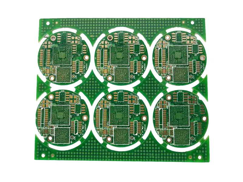
The core principle of PCB shape panelization lies in material utilization, where geometry determines how densely boards fit within the panel boundary. Rectangular forms allow orthogonal arrays with minimal interstitial space, often achieving over high utilization rates through simple replication. Complex shapes, however, create voids when tiled, as curved or angled perimeters fail to nest perfectly without rotation or spacing adjustments. This geometric mismatch directly scales production costs proportional to panel area.
Depaneling mechanics further highlight shape disparities. V-scoring, ideal for rectangular PCB panelization, etches partial-depth grooves along straight axes, enabling clean snap-separation with controlled force. The process aligns with board thickness uniformity, distributing stress evenly to avoid warpage. For irregular PCBs, V-scoring becomes impractical due to non-linear edges, shifting reliance to mechanical routing or laser depaneling, which generate heat and vibration that can propagate into copper layers.
Stress analysis reveals additional risks with complex contours. During tab routing depaneling, localized forces at holding points induce bending moments, particularly acute on thin flex areas of irregular boards. Engineering simulations model these as cantilever loads, where contour radius influences failure thresholds. Adhering to IPC-A-600 acceptability criteria ensures post-depanel edges meet surface quality standards, mitigating risks like burrs or fiber exposure.
Thermal effects compound these issues during reflow soldering. Panels of rectangular boards maintain flatness better under JEDEC J-STD-020 guidelines for moisture sensitivity, as uniform expansion matches panel rails. Irregular arrays experience differential contraction, exacerbating bow and twist. Optimizing space for complex shapes via rotated orientations in arrays helps, but requires validation through shadow moire analysis or dial gauge measurements.
Handling and tooling tolerances tie back to shape as well. Factory panels standardize at fixed dimensions, so protruding contours demand buffer zones, reducing effective yield. CAD software panelization algorithms address this by computing tessellations that minimize perimeter overlap, factoring in rail widths and fiducial placements.
Best Practices for Rectangular PCB Panelization
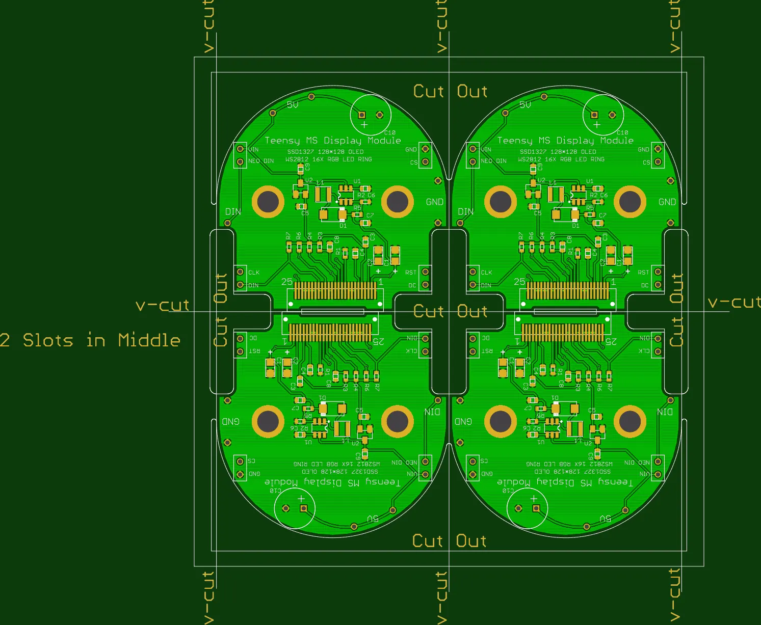
For rectangular boards, prioritize V-scoring to capitalize on shape simplicity. Design grooves to span full board lengths, maintaining consistent depth relative to substrate thickness for reliable fracturing. Incorporate breakaway rails at least wide enough for fixture grips, positioning them opposite scoring lines to balance panel rigidity. This setup supports automated inline processing without compromising alignment.
Spacing between boards should accommodate tooling clearance while maximizing density. Uniform arrays prevent asymmetric loading during lamination or plating, preserving layer registration. Include tooling holes and fiducials symmetrically to aid optical recognition in assembly.
Depaneling preparation involves perforating score lines partially if snap-risk exists, blending with mouse bites for hybrid strength. Post-separation inspection verifies edge straightness per IPC standards, ensuring no chipping propagates inward. Electrical engineers benefit from simulating fracture propagation in design phases to preempt issues.
Validate panel flatness pre-assembly, as rectangular configurations inherently resist warpage better than alternatives.
Best Practices for Panelizing Irregular PCBs
Panelizing irregular PCBs demands tab routing primacy, with perforations or mouse bites securing boards to the frame. Strategically place tabs at structurally robust locations, avoiding high-density component zones or trace runs to isolate depaneling stresses. Contour routing paths should arc smoothly, minimizing tool marks and heat-affected zones that could warp thin sections.
Optimizing space for complex shapes relies on CAD software panelization features. Rotate alternating rows by 90 or 180 degrees to tessellate protrusions into adjacent voids, boosting utilization beyond naive grids. Iterative algorithms in these tools compute optimal arrays, outputting Gerber files with embedded rails and break lines.
Hybrid methods combine tabs with partial V-scores on straight segments, hybridizing efficiency. Factory protocols emphasize pilot runs to tune router feeds, preventing vibration-induced microcracks. Edge chamfers on contours enhance handling safety post-depanel.
Fiducials must cluster accessibly, compensating for shape-induced asymmetry in vision systems.
Case Insights: Rectangular vs. Complex in Practice
Consider a production run contrasting a rectangular sensor board with an L-shaped enclosure interface PCB. The rectangular design panels into a 4x5 array via V-scoring, yielding compact processing and snap-depaneling under 50N force. Material use hovers efficiently, with rails reclaimable for scrap reduction.
The L-shaped counterpart requires tab-routed 3x4 panel, rotated 90 degrees in even rows to fill bays, yet still incurs 20 percent more waste. Depaneling shifts to milling, introducing 10-minute cycle extensions per panel. Yield holds steady, but inspection time rises due to contour variability.
These insights affirm rectangular preference for volume, while CAD-driven optimization salvages irregular viability. Engineers weigh enclosure demands against fab economics accordingly.
Conclusion
PCB shape profoundly shapes panelization strategies, with rectangles enabling efficient V-scoring and dense arrays, while complex contours necessitate tab routing and spatial tweaks. Technical principles of utilization, stress, and thermal stability underscore these trade-offs, guided by standards like IPC-2221 and JEDEC J-STD-020. Best practices in CAD software panelization empower engineers to mitigate inefficiencies, ensuring cost-effective manufacturing. Prioritizing shape awareness from design onset optimizes outcomes across the production chain.
FAQs
Q1: What are the main differences in rectangular PCB panelization versus panelizing irregular PCBs?
A1: Rectangular PCB panelization favors V-scoring for straight-line separation and high material efficiency, aligning with uniform handling. Panelizing irregular PCBs relies on tab routing or mouse bites to accommodate contours, often requiring rotated layouts to optimize space. These methods introduce more stress points, demanding careful tab placement per design guidelines. Overall, rectangles streamline volume production, while irregulars suit custom fits with added planning.
Q2: How does PCB shape affect material utilization in panelization?
A2: PCB shape panelization efficiency stems from tiling geometry; rectangles pack orthogonally with minimal waste. Complex shapes create gaps unless CAD software panelization rotates boards to nest protrusions. This optimization can recover 10-20 percent space but complicates routing paths. Factory metrics track panel yield to quantify impacts, guiding design revisions.
Q3: What role does CAD software play in optimizing space for complex shapes?
A3: CAD software panelization automates array computation for irregular PCBs, testing rotations and spacings to maximize density. It generates production-ready outputs with rails, fiducials, and depanel lines tailored to contours. Engineers input constraints like tab counts, yielding simulations that predict utilization and stress. This tool bridges design intent with fab feasibility.
Q4: Why consider depaneling stress when choosing panelization for different PCB shapes?
A4: Depaneling stress varies by shape; V-scoring distributes loads evenly on rectangles, per IPC-A-600 criteria. Irregulars concentrate forces at tabs, risking delamination without reinforcements. Preemptive modeling ensures acceptability, especially post-reflow. Balanced strategies maintain integrity across shapes.
References
IPC-2221B — Generic Standard on Printed Board Design. IPC, 2003
IPC-A-600K — Acceptability of Printed Boards. IPC, 2020
JEDEC J-STD-020E — Moisture/Reflow Sensitivity Classification. JEDEC, 2014