 ALLPCB


Are you struggling with reflow soldering defects in your PCB assembly process? Issues like solder bridging, tombstoning, and solder balling can compromise the quality and reliability of your electronic products. In this comprehensive reflow soldering troubleshooting guide, we’ll explore the common causes of reflow soldering defects and provide practical solutions to help you achieve flawless solder joints. Whether you’re a seasoned electrical engineer or new to surface mount technology (SMT), this guide will equip you with the knowledge to tackle these challenges head-on.
Introduction to Reflow Soldering and Its Importance
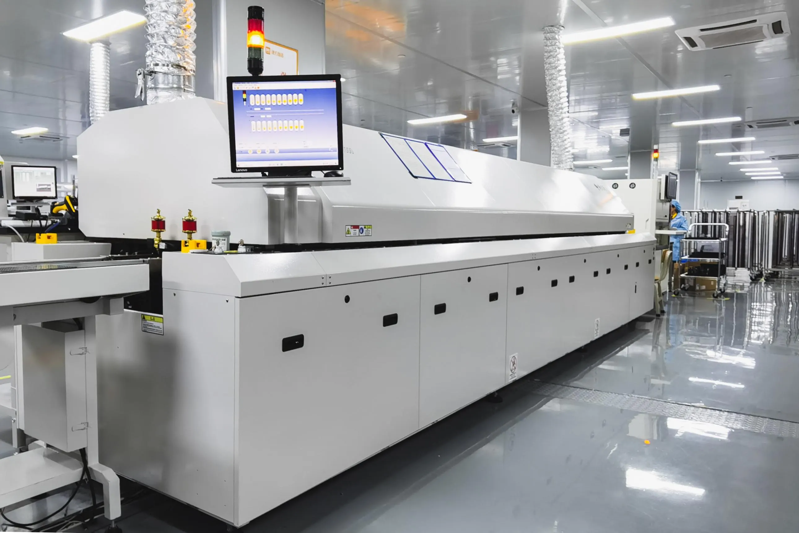
Reflow soldering is a critical process in modern electronics manufacturing, especially for surface mount technology (SMT). It involves applying solder paste to a printed circuit board (PCB), placing components, and heating the assembly in a reflow oven to melt the solder and form strong electrical and mechanical connections. When done correctly, reflow soldering ensures reliable joints and high-quality PCB assemblies. However, defects can occur due to various factors, leading to costly rework or product failures.
As an electrical engineer, understanding the causes of reflow soldering defects and knowing how to troubleshoot them is essential for maintaining production efficiency and product reliability. In this blog, ALLPCB will dive deep into the most common issues—solder bridging, tombstoning, and solder balling—and offer actionable solutions to prevent and fix them.
What Are the Most Common Reflow Soldering Defects?
Before we explore the causes and solutions, let’s identify the most frequent reflow soldering defects encountered in PCB assembly. These issues can disrupt functionality and require careful attention to resolve:
- Solder Bridging: Unwanted connections between adjacent pads or leads due to excess solder forming a bridge.
- Tombstoning: A component standing upright on one end, resembling a tombstone, due to uneven soldering.
- Solder Balling: Small, unintended balls of solder forming on the PCB surface, risking short circuits.
Each of these defects has specific causes tied to materials, processes, or equipment. Let’s break them down one by one, focusing on reflow soldering defects causes and solutions.
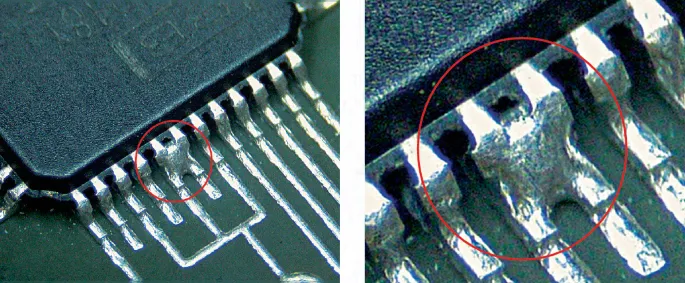
1. Solder Bridging: Causes and Solutions
What Causes Solder Bridging?
Solder bridging occurs when excess solder creates an unintended connection between two or more adjacent pads or pins, often leading to short circuits. Common causes include:
- Excess Solder Paste: Over-applying solder paste during stencil printing can cause it to spread and connect neighboring pads during reflow.
- Incorrect Stencil Design: A stencil with apertures that are too large or poorly aligned can deposit excessive paste in the wrong areas.
- Improper Reflow Profile: A temperature profile that heats too quickly or unevenly can cause solder to flow uncontrollably.
- Component Misalignment: Misplaced components can bring pads closer together, increasing the risk of bridging.
Solutions to Prevent Solder Bridging
To address solder bridging, engineers can take the following steps:
- Optimize Stencil Design: Ensure stencil apertures are appropriately sized (typically 80-90% of pad size) and aligned with the PCB layout. Regularly inspect stencils for wear or damage.
- Control Solder Paste Volume: Use a stencil thickness of 0.1-0.15 mm for fine-pitch components to avoid over-deposition. Employ automated solder paste inspection (SPI) systems to verify paste volume before reflow.
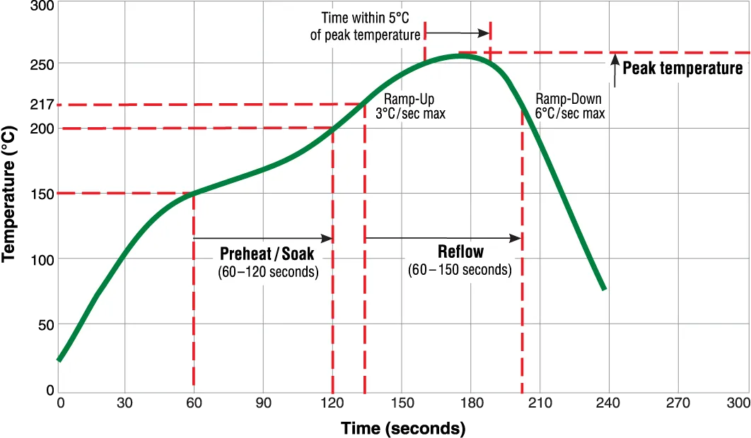
- Adjust Reflow Profile: Set a gradual ramp-up rate (1-3°C per second) in the preheat zone to avoid rapid solder melting. Ensure peak temperatures (typically 235-250°C for lead-free solder) are not exceeded.
- Verify Component Placement: Use high-precision pick-and-place machines to ensure components are placed accurately, minimizing the risk of misalignment.
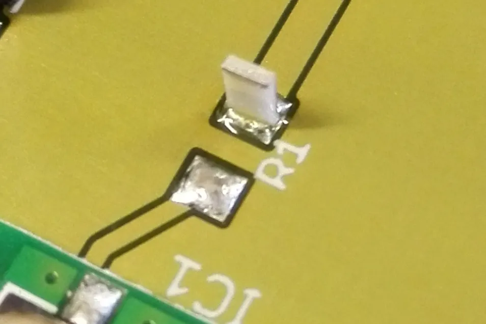
2. Tombstoning: Causes and Solutions
What Causes Tombstoning?
Tombstoning happens when a component lifts on one end during reflow, standing vertically like a tombstone. This defect often affects small passive components like resistors and capacitors. Key causes include:
- Uneven Heating: If one side of a component heats faster than the other, the solder on that side melts first, pulling the component upright due to surface tension.
- Pad Size Discrepancy: Unequal pad sizes or shapes under a component can lead to uneven solder wetting.
- Insufficient Solder Paste: Too little paste on one pad can prevent proper adhesion, causing the component to tilt.
- Component Placement Issues: Poor placement accuracy or excessive pressure during placement can misalign components, contributing to tombstoning.
Solutions to Prevent Tombstoning
Here are practical steps to mitigate tombstoning in your reflow soldering process:
- Balance Reflow Profile: Design a reflow profile with a preheat zone (150-180°C for 60-90 seconds) to ensure even heating across the PCB. Avoid rapid temperature spikes that can cause uneven melting.
- Standardize Pad Design: Ensure pads under components are symmetrical in size and shape. Follow IPC standards (e.g., IPC-7351) for pad dimensions to promote uniform solder wetting.
- Check Solder Paste Deposition: Use SPI tools to confirm consistent paste volume on both pads of a component. Aim for a paste height of 0.12-0.15 mm for small components.
- Improve Placement Accuracy: Calibrate pick-and-place machines to achieve placement accuracy within ±0.05 mm. Minimize mechanical stress during component placement.
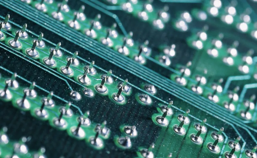
3. Solder Balling: Causes and Solutions
What Causes Solder Balling?
Solder balling refers to the formation of small, spherical solder beads on the PCB surface or near solder joints. These balls can cause short circuits if they move during operation. Common causes include:
- Moisture in Solder Paste: Trapped moisture can vaporize during reflow, creating splatter and forming solder balls.
- Excessive Solder Paste: Too much paste can lead to overflow, resulting in stray solder beads.
- Inadequate Reflow Profile: A profile with insufficient preheat time or low temperatures can prevent proper solder coalescence, leading to balling.
- PCB Contamination: Residues or dirt on the PCB surface can interfere with solder flow, causing balls to form.
Solutions to Prevent Solder Balling
Combat solder balling with these targeted solutions:
- Store Solder Paste Properly: Keep solder paste refrigerated at 2-10°C and allow it to reach room temperature (20-25°C) for 4-6 hours before use to prevent moisture condensation.
- Control Paste Application: Use a stencil with precise apertures and inspect paste deposits to ensure they match design specifications (e.g., 0.1-0.15 mm thickness for fine-pitch applications).
- Optimize Reflow Profile: Extend the preheat zone to 60-120 seconds at 150-180°C to evaporate moisture and promote even solder flow. Avoid peak temperatures below the solder’s melting point (e.g., 217°C for SAC305 lead-free solder).
- Clean PCBs Thoroughly: Use isopropyl alcohol or specialized PCB cleaners to remove contaminants before applying solder paste. Implement a no-clean flux if contamination persists post-reflow.
General Reflow Soldering Troubleshooting Guide
Beyond specific defects, a systematic approach to troubleshooting reflow soldering issues can save time and resources. Follow this step-by-step guide to diagnose and resolve problems in your assembly process:
- Inspect Visual Defects: Use a magnifying glass or AOI inspection to identify visible issues like bridging, tombstoning, or solder balling after reflow.
- Review Reflow Profile: Check temperature settings and zone durations using a thermal profiler. Ensure the profile matches the solder paste manufacturer’s recommendations (e.g., peak temperature 20-40°C above melting point for 30-60 seconds).
- Evaluate Solder Paste Quality: Verify the paste’s shelf life and storage conditions. Test for viscosity (typically 600-800 kcps for type 3 paste) to ensure it’s suitable for printing.
- Assess PCB and Component Condition: Look for contamination, oxidation, or damage on PCB pads and component leads. Replace or clean as needed.
- Analyze Equipment Performance: Calibrate the reflow oven for uniform heat distribution (within ±5°C across zones) and verify stencil printer accuracy for consistent paste deposition.
- Document and Iterate: Record findings and adjustments after each troubleshooting cycle. Test small batches to confirm solutions before scaling up production.
Best Practices for Preventing Reflow Soldering Defects
Prevention is always better than rework. Implement these best practices to minimize reflow soldering defects in your workflow:
- Use High-Quality Materials: Select solder paste and components from reputable suppliers with consistent performance specifications.
- Adhere to IPC Standards: Follow guidelines like IPC-A-610 for acceptable solder joint criteria and IPC-J-STD-001 for soldering processes.
- Maintain Equipment: Regularly clean and calibrate reflow ovens, stencil printers, and pick-and-place machines to ensure precision.
- Train Personnel: Educate your team on proper handling of materials, equipment setup, and defect identification to reduce human error.
- Implement Inspection Systems: Use SPI and AOI to catch issues early in the process, reducing the likelihood of defects reaching final assembly.
Conclusion: Mastering Reflow Soldering for Reliable PCB Assemblies
Reflow soldering defects like solder bridging, tombstoning, and solder balling can be frustrating, but with the right knowledge and tools, they are entirely manageable. By understanding the root causes—whether it’s an improper reflow profile, stencil design issues, or material quality—and applying targeted solutions, electrical engineers can achieve high-quality, reliable PCB assemblies. Use this reflow soldering troubleshooting guide as your go-to resource for diagnosing and fixing issues in your production line.
Remember, consistency is key. Regularly monitor your process parameters, invest in quality control systems, and stay updated on industry best practices to keep defects at bay.


