 ALLPCB


If you're working on a Surface Mount Technology (SMT) PCB layout, avoiding Design for Assembly (DFA) mistakes is crucial to ensure a smooth manufacturing process and a reliable final product. SMT assembly problems can lead to costly delays, rework, or even product failures. In this blog post, we'll dive into the top 5 DFA mistakes in SMT PCB layout errors, helping you sidestep common pitfalls and optimize your design for efficient production. Whether you're a seasoned engineer or new to PCB design, understanding these common DFA errors in PCB layouts can save you time and resources.
Let's explore these mistakes in detail, with actionable tips and insights to improve your SMT PCB layout process and avoid costly errors.
Why Design for Assembly Matters in SMT PCB Layout
Design for Assembly (DFA) focuses on creating PCB layouts that are easy and cost-effective to manufacture. In SMT, where components are mounted directly onto the surface of the board, small design oversights can lead to significant assembly challenges. SMT assembly problems often stem from poor planning in the layout stage, resulting in issues like misaligned components, soldering defects, or even complete assembly failures.
By addressing common DFA errors in PCB design early, you can reduce manufacturing costs, improve yield rates, and ensure your product meets performance expectations. Let’s break down the top 5 PCB design pitfalls to avoid in SMT layouts and how to tackle them effectively.
Mistake 1: Insufficient Component Spacing
One of the most frequent SMT PCB layout errors is placing components too close together. While it might seem efficient to pack components tightly to save board space, this often leads to assembly challenges. Insufficient spacing can prevent automated pick-and-place machines from accurately positioning components, increasing the risk of misalignment or damage during assembly.
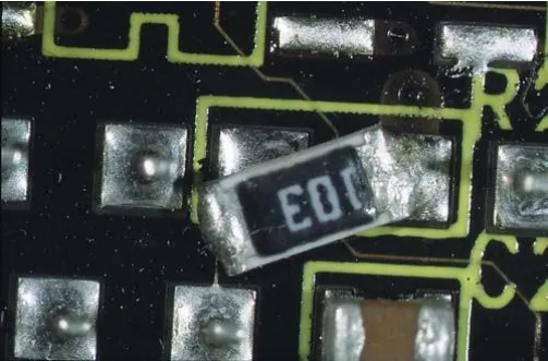
Moreover, tight spacing can cause issues during soldering. For instance, if components are placed less than 0.5 mm apart, solder paste may bridge between pads, leading to short circuits. This is especially problematic in high-density designs where fine-pitch components, like 0.4 mm pitch QFNs, are common.
How to Avoid This Mistake: Always follow the recommended spacing guidelines provided in component datasheets. As a general rule, maintain at least 0.8 mm to 1 mm of clearance between SMT components for standard designs. For high-density boards, use design software with built-in design rule checks (DRC) to flag spacing violations before sending your design to production.
Mistake 2: Incorrect Footprint Design
Another common DFA error in PCB design is using incorrect or mismatched footprints for SMT components. A footprint defines the pad size, shape, and spacing where a component is soldered to the board. If the footprint doesn’t match the physical dimensions of the component, it can result in poor solder joints, misalignment, or components not fitting at all.
For example, using a footprint designed for a 0603 resistor (1.6 mm x 0.8 mm) when your design calls for a smaller 0402 resistor (1.0 mm x 0.5 mm) can lead to soldering defects. These errors often go unnoticed until the assembly stage, causing delays and rework.
How to Avoid This Mistake: Double-check the footprint against the component datasheet before finalizing your layout. Use library components from trusted sources or create custom footprints with precise measurements. Additionally, run a pre-assembly verification using 3D modeling tools in your design software to ensure the footprint matches the component's physical dimensions.
Mistake 3: Poor Placement of Fiducial Marks
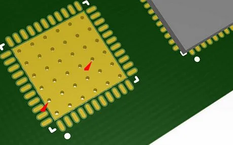
Fiducial marks are reference points on a PCB that help automated assembly machines align components accurately during SMT assembly. A common PCB design pitfall is neglecting to include fiducial marks or placing them in suboptimal locations. Without clear fiducials, pick-and-place machines may struggle to orient the board correctly, leading to component misalignment and assembly errors.
For instance, if fiducials are placed too close to the board edge (less than 5 mm), they may be obscured by clamps or fixtures during assembly. Similarly, placing fiducials near large components can interfere with the machine's vision system.
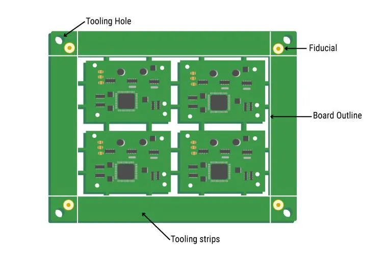
How to Avoid This Mistake: Include at least two fiducial marks on opposite corners of the PCB, ideally 1.0 mm in diameter with a 2.0 mm clearance zone around them. Position them away from board edges and large components to ensure visibility. If your design includes panels, add fiducials on the panel frame as well for accurate alignment during mass production.
Mistake 4: Ignoring Thermal Management in Layout
Thermal management is often overlooked in SMT PCB layouts, leading to overheating issues during operation or assembly. Components like power ICs, LEDs, or high-current resistors generate significant heat, and without proper heat dissipation, solder joints can weaken or components may fail prematurely. A common DFA mistake in SMT is failing to provide adequate thermal relief or vias for heat dissipation.
For example, a power MOSFET generating 5W of heat on a board without thermal vias may cause the local temperature to rise above 100°C, risking damage to nearby components. Poor thermal design can also cause uneven heating during reflow soldering, leading to defects like tombstoning, where one end of a component lifts off the pad.
How to Avoid This Mistake: Incorporate thermal vias under high-heat components to transfer heat to other layers or a heatsink. Use copper pours connected to ground planes to spread heat evenly across the board. Additionally, follow the component datasheet for recommended thermal pad sizes—often 1.5 to 2 times larger than the component itself for effective heat dissipation.
Mistake 5: Inadequate Solder Mask and Silkscreen Design
The solder mask and silkscreen layers play a vital role in SMT assembly, yet they are often neglected in PCB design. A poorly designed solder mask can expose unintended copper areas, leading to solder bridging or shorts during reflow. Similarly, unclear or missing silkscreen markings can confuse assemblers, especially during manual inspection or rework, contributing to SMT assembly problems.
For instance, if the solder mask opening for a 0.5 mm pitch BGA is too large, excess solder paste may cause bridging between pins. On the silkscreen side, omitting polarity indicators for diodes or capacitors can lead to incorrect component orientation during assembly.
How to Avoid This Mistake: Ensure the solder mask openings are slightly larger than the pads—typically by 0.1 mm on each side—to prevent solder paste from spreading. For silkscreen, include clear markings for component orientation, reference designators, and pin 1 indicators for ICs. Use design rule checks to verify solder mask clearances and silkscreen readability before fabrication.
Additional Tips to Prevent DFA Mistakes in SMT PCB Layout
Beyond these top 5 mistakes, here are a few additional strategies to refine your SMT PCB layout and minimize common DFA errors:
- Use Design Rule Checks (DRC): Leverage DRC tools in your PCB design software to catch spacing, footprint, and clearance issues early. Set rules based on your manufacturer’s capabilities, such as minimum trace widths of 0.15 mm for standard processes.
- Collaborate with Your Manufacturer: Share your design files with your assembly partner during the planning stage. They can provide feedback on potential SMT assembly problems based on their equipment and processes.
- Test with Prototypes: Before full-scale production, build a prototype to identify layout issues. For instance, test reflow soldering profiles to ensure components like 0201 capacitors (0.6 mm x 0.3 mm) don’t tombstone due to uneven heating.
The Impact of Avoiding DFA Mistakes in SMT PCB Layout
By steering clear of these common DFA errors in PCB design, you can significantly improve the manufacturability of your SMT boards. Proper spacing, accurate footprints, fiducial placement, thermal management, and solder mask design directly contribute to higher assembly yields—often increasing first-pass success rates from 85% to over 95% in some cases. This not only reduces production costs but also speeds up time-to-market for your products.
Moreover, a well-designed SMT PCB layout minimizes the risk of field failures due to soldering defects or thermal stress. For engineers working on high-reliability applications, such as medical or automotive electronics, avoiding these PCB design pitfalls is non-negotiable.
Conclusion: Optimize Your SMT PCB Layout for Success
Designing an SMT PCB layout that adheres to DFA principles is a critical step in ensuring a seamless assembly process and a high-quality end product. By addressing the top 5 DFA mistakes—insufficient spacing, incorrect footprints, poor fiducial placement, inadequate thermal management, and flawed solder mask or silkscreen design—you can avoid common SMT PCB layout errors and enhance production efficiency.
Take the time to review your designs, incorporate manufacturer feedback, and use advanced tools to catch errors early. With careful planning and attention to detail, you can overcome SMT assembly problems and deliver reliable, cost-effective PCBs for any application. Start optimizing your layouts today to stay ahead of potential pitfalls and achieve better results in your next project.


