 ALLPCB


If you're looking to optimize your printed circuit board (PCB) designs for high-density interconnect (HDI) assembly, via-in-pad technology might be the game-changer you need. But what exactly is via-in-pad in HDI assembly, and why should you consider it? In short, via-in-pad technology involves placing vias directly under component pads, allowing for tighter layouts, improved thermal management, and better signal integrity in compact designs. This guide dives deep into the world of via-in-pad HDI assembly, exploring its advantages like VIPPO (via-in-pad plated over), thermal management benefits, routing techniques, and how it helps increase component density. Let’s explore how this innovative approach can elevate your PCB projects.
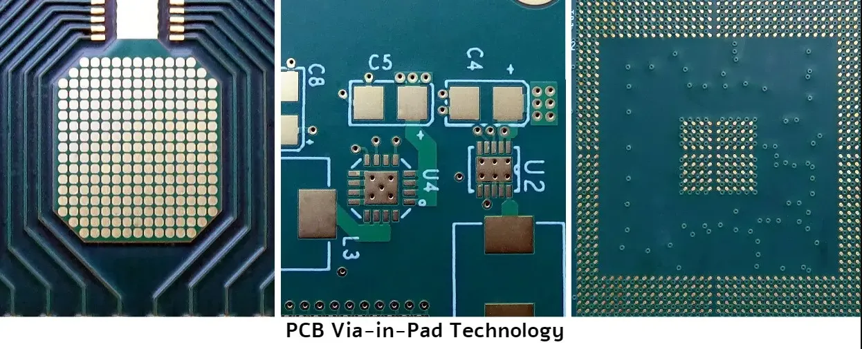
What Is Via-in-Pad Technology in HDI Assembly?
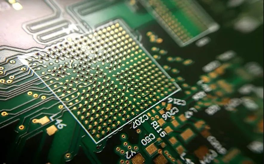
Via-in-pad technology is a design technique used in HDI assembly where vias—small holes that connect different layers of a PCB—are placed directly beneath the pads of surface-mount components. Unlike traditional vias, which are positioned outside the component pads and take up additional board space, via-in-pad integrates these connections into the pad itself. This method is often paired with a process called VIPPO (via-in-pad plated over), where the via is filled and plated to create a flat surface for component mounting.
In HDI assembly, where space is at a premium, this technology allows for finer pitch components and more compact designs. It’s especially useful for modern electronics like smartphones, wearables, and IoT devices, which demand high performance in tiny footprints. By eliminating the need for extra space around vias, designers can pack more functionality into smaller areas, directly addressing the need for component density increase.
Key Advantages of Via-in-Pad Technology in HDI Assembly
The benefits of via-in-pad technology, especially when combined with VIPPO, make it a go-to choice for advanced PCB designs. Here are the standout advantages that can transform your HDI projects.
1. Space Savings and Component Density Increase
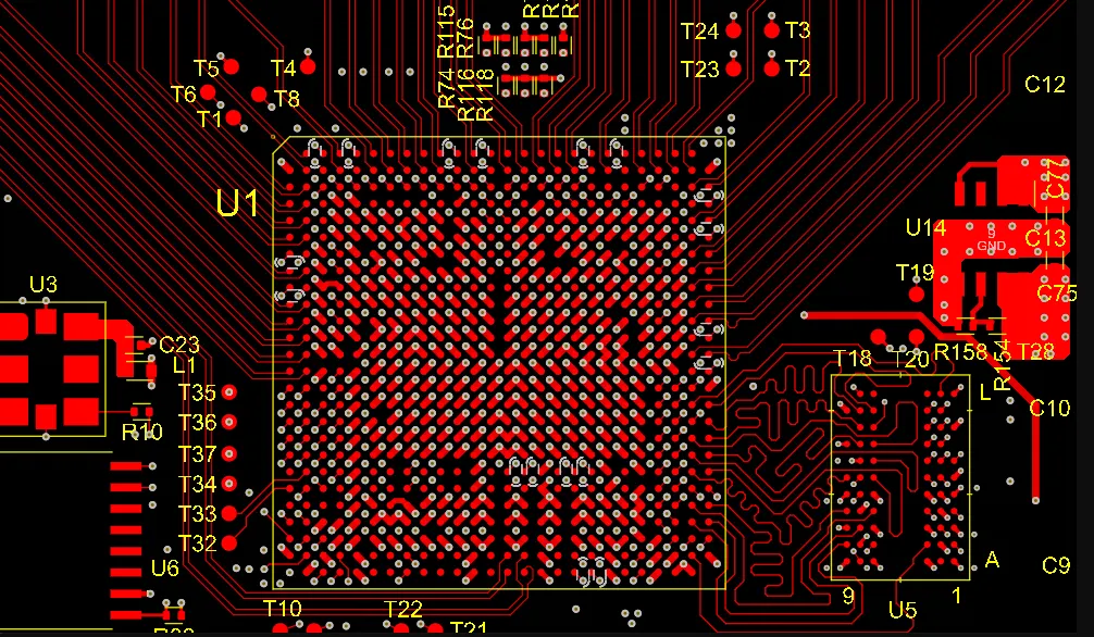
One of the most significant perks of via-in-pad HDI assembly is the ability to drastically reduce the space needed on the PCB. Traditional via placement requires additional room for traces to route around vias, often leading to larger board sizes. With via-in-pad, you can place vias directly under components, freeing up valuable real estate. This allows for a notable component density increase, enabling designs with finer pitch components like 0.4mm or even 0.3mm ball grid arrays (BGAs). For instance, in a typical HDI design for a smartphone, this can mean fitting 20-30% more components in the same area compared to conventional layouts.
2. Improved Signal Integrity
In high-speed designs, signal integrity is critical. Via-in-pad technology minimizes the length of traces needed to connect components to vias, reducing parasitic inductance and capacitance. Shorter traces mean less signal delay and lower risk of crosstalk. For example, in a design operating at 5 GHz, reducing trace length by just a few millimeters through via-in-pad can cut signal delay by up to 10 picoseconds, ensuring cleaner data transmission.
3. Enhanced Thermal Management with Via-in-Pad
Thermal management via-in-pad is another major advantage. Placing vias directly under heat-generating components, such as power ICs or processors, creates a direct path for heat to dissipate through the PCB layers to a heat sink or ground plane. This can lower the operating temperature of critical components by 5-10°C in some designs, extending their lifespan and reliability. In HDI boards with multiple layers, vias can be strategically placed to form thermal conduits, efficiently managing heat in compact spaces.
4. VIPPO Advantages: Reliability and Manufacturability
The VIPPO (via-in-pad plated over) process enhances the benefits of via-in-pad by filling the via with conductive material and plating over it to create a smooth, flat surface. This eliminates the risk of solder wicking into the via during assembly, which can cause voids or weak joints. VIPPO also improves the structural integrity of the pad, making it more robust for component placement. The result is a more reliable board with fewer assembly defects—critical for high-stakes applications like medical devices or automotive electronics.
Thermal Management Via-in-Pad: A Closer Look
Heat dissipation is a constant challenge in modern electronics, especially as devices get smaller and more powerful. Thermal management via-in-pad offers a practical solution by turning vias into heat conduits. When placed under high-power components, these vias transfer heat directly to inner layers or ground planes, which can act as thermal sinks. This is particularly effective in multilayer HDI boards, where heat can be spread across several planes.
For example, in a design with a power IC generating 3W of heat, adding multiple thermal vias under the component pad can reduce junction temperature by up to 8°C. The key is to use an array of vias—often 4 to 8 under a single pad—combined with a copper-filled structure for maximum conductivity. Designers should also ensure the vias connect to a large copper area on the opposite side of the board to enhance heat spreading.
However, it’s important to balance thermal vias with electrical needs. Too many vias can interfere with signal routing or ground plane integrity. Using simulation tools to model heat flow and optimize via placement can help strike this balance, ensuring both thermal performance and electrical reliability.
HDI Routing Techniques with Via-in-Pad
Routing in HDI designs is complex due to the high component density and limited space. Via-in-pad technology, paired with advanced HDI routing techniques, offers solutions to these challenges. Here’s how it works and some strategies to maximize its potential.
1. Microvia Integration
HDI boards often use microvias—tiny vias with diameters as small as 0.1mm—to connect layers. When combined with via-in-pad, microvias allow for precise routing directly under components, minimizing trace lengths. This is ideal for fine-pitch BGAs, where escape routing (connecting inner pins to outer layers) can be a bottleneck. For instance, a 0.5mm pitch BGA with 256 pins can be routed using microvias under pads, reducing the need for additional layers by up to 2 in some designs.
2. Stacked and Staggered Vias
In multilayer HDI boards, stacked or staggered vias can enhance routing flexibility. Stacked vias connect multiple layers directly under a pad, while staggered vias offset connections to avoid interference. Using via-in-pad with these techniques ensures efficient use of space while maintaining signal integrity. Designers must ensure proper via aspect ratios (depth-to-diameter) are maintained—typically below 0.8:1 for microvias—to avoid manufacturing issues.
3. Fan-Out Optimization
For complex components like BGAs or QFNs, fan-out routing is critical. Via-in-pad allows for direct fan-out under the component, reducing the number of vias needed outside the footprint. This not only saves space but also simplifies the routing process, cutting design time and potential errors. Software tools with auto-routing features can help optimize these layouts, ensuring traces are as short and direct as possible.
Challenges of Via-in-Pad in HDI Assembly
While via-in-pad technology offers numerous benefits, it’s not without challenges. Understanding these hurdles can help designers make informed decisions and avoid pitfalls.
1. Manufacturing Complexity
Implementing via-in-pad, especially with VIPPO, adds complexity to the manufacturing process. Filling and plating vias require precise control to avoid defects like voids or uneven surfaces. This can increase production costs by 10-15% compared to standard HDI processes. Working with a reliable fabrication partner who has experience in advanced HDI techniques is essential to ensure quality.
2. Design Constraints
Via-in-pad placement must be carefully planned to avoid interfering with component performance. For example, placing too many vias under a pad can weaken its structural integrity, leading to issues during soldering. Designers should follow guidelines like maintaining a minimum via-to-pad edge distance (often 0.1mm) and limiting via density based on pad size.
3. Thermal and Electrical Trade-Offs
While thermal management via-in-pad is a major advantage, overusing thermal vias can disrupt ground planes or signal paths, causing electrical noise. Balancing thermal and electrical requirements through simulation and testing is crucial to achieving optimal performance.
Best Practices for Implementing Via-in-Pad in HDI Designs
To make the most of via-in-pad technology in HDI assembly, follow these best practices for design and manufacturing success.
- Optimize Via Size and Placement: Use microvias with diameters of 0.1-0.15mm for space savings, and place them strategically under pads to avoid mechanical stress on components.
- Use VIPPO for Reliability: Opt for via-in-pad plated over techniques to prevent solder wicking and ensure a flat mounting surface, especially for fine-pitch components.
- Simulate Thermal and Signal Performance: Leverage design software to model heat dissipation and signal integrity, ensuring vias enhance performance without causing interference.
- Collaborate with Fabricators: Work closely with your PCB manufacturer to align design rules with their capabilities, minimizing production risks and costs.
Conclusion: Why Via-in-Pad Is the Future of HDI Assembly
Via-in-pad technology is revolutionizing HDI assembly by offering unparalleled space savings, improved thermal management, and enhanced signal integrity. From enabling component density increase to optimizing HDI routing techniques, this approach addresses the demands of modern electronics with precision and efficiency. The VIPPO advantages further boost reliability, making it a trusted choice for high-performance applications.
By understanding its benefits and challenges, and following best practices, designers can harness the full potential of via-in-pad in their projects. Whether you're working on a cutting-edge wearable device or a complex automotive system, this technology can help you achieve smaller, faster, and more reliable designs. Embrace via-in-pad HDI assembly to stay ahead in the ever-evolving world of PCB design.


