 ALLPCB


In the world of modern electronics, High-Density Interconnect (HDI) assembly has become a cornerstone for creating compact, high-performance devices. But how do you ensure high signal integrity in such tight spaces? The key lies in meticulous design practices focusing on impedance control, crosstalk reduction, strategic signal layer placement, and tailored approaches for high-frequency applications. This blog dives deep into the essentials of HDI assembly signal integrity, offering practical tips and insights to help engineers achieve reliable performance in compact designs.
What is HDI Assembly and Why Does Signal Integrity Matter?
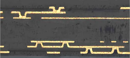
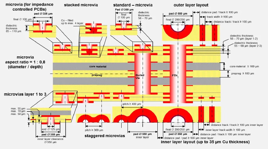
HDI assembly refers to the process of building printed circuit boards (PCBs) with a higher wiring density per unit area compared to traditional boards. These designs often use microvias, blind vias, and buried vias to pack more functionality into smaller spaces, making them ideal for smartphones, wearables, and other compact devices. However, the reduced size and increased complexity come with challenges, especially in maintaining signal integrity.
Signal integrity refers to the quality of an electrical signal as it travels through a circuit. Poor signal integrity can lead to data loss, delays, or system failures due to issues like noise, crosstalk, or impedance mismatches. In HDI designs, where traces are closer together and layers are stacked tightly, achieving high signal integrity is critical to ensure the device operates as intended.
In this post, we’ll explore proven strategies for optimizing HDI assembly signal integrity, focusing on impedance control in HDI, crosstalk reduction in HDI, signal layer placement, and high-frequency HDI design. Let’s get started with the foundational elements.
Understanding Signal Integrity Challenges in HDI Assembly
HDI boards are designed for compactness, which means shorter trace lengths and tighter spacing. While this saves space, it introduces several signal integrity challenges:
- Impedance Mismatches: Variations in trace width, dielectric material, or layer thickness can disrupt signal transmission, causing reflections and signal loss.
- Crosstalk: Close proximity of traces increases the risk of electromagnetic interference between adjacent signals, leading to data corruption.
- High-Frequency Issues: At higher frequencies (e.g., above 1 GHz), signal loss due to dielectric properties and skin effect becomes more pronounced.
- Power Distribution Noise: Compact designs often struggle with providing stable power delivery, leading to noise that affects signal quality.
Addressing these challenges requires a combination of design techniques and material choices. Let’s break down the key strategies for maintaining HDI assembly signal integrity.
Impedance Control in HDI: The Backbone of Signal Integrity
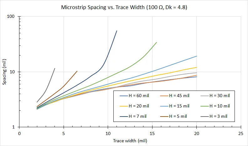
Impedance control in HDI is one of the most critical factors for ensuring signals travel without distortion. Impedance, measured in ohms, must be consistent along a trace to prevent reflections. For high-speed signals, a common target impedance is 50 ohms for single-ended traces and 100 ohms for differential pairs.
To achieve impedance control in HDI designs, consider the following:
- Trace Width and Spacing: Use precise calculations to determine trace width based on the dielectric constant (Dk) of the material and the desired impedance. For example, a 50-ohm trace on a standard FR-4 material with a Dk of 4.2 might require a width of around 6 mils at a specific layer thickness.
- Dielectric Material Selection: Choose materials with consistent Dk values and low loss tangent for high-frequency HDI designs. Advanced laminates with Dk values between 3.0 and 3.5 are often preferred over standard FR-4 for better performance at frequencies above 5 GHz.
- Layer Stack-Up Design: Plan the stack-up to maintain symmetry and control impedance. Place ground planes adjacent to signal layers to provide a stable reference and minimize variations.
Simulation tools can help predict impedance before manufacturing, allowing designers to adjust trace geometries and material choices. By prioritizing impedance control in HDI, you can significantly reduce signal reflections and improve overall performance.
Crosstalk Reduction in HDI: Minimizing Signal Interference
Crosstalk reduction in HDI is essential due to the close proximity of traces in compact layouts. Crosstalk occurs when electromagnetic fields from one trace interfere with a neighboring trace, causing noise and potential data errors. This issue becomes more severe at higher frequencies and with tighter trace spacing.
Here are actionable tips for crosstalk reduction in HDI designs:
- Increase Trace Spacing: Maintain a minimum spacing of at least 3 times the trace width between adjacent high-speed signals to reduce coupling. For example, if a trace is 5 mils wide, aim for a spacing of 15 mils or more.
- Use Ground Planes: Place continuous ground planes between signal layers to act as a shield, absorbing stray electromagnetic fields. This is particularly effective in multi-layer HDI stack-ups.
- Route Signals Orthogonally: On adjacent layers, route high-speed signals perpendicular to each other to minimize overlap and coupling.
- Differential Pair Routing: For high-speed differential signals, keep the pair tightly coupled and maintain equal lengths to reduce susceptibility to crosstalk.
By implementing these strategies, you can effectively manage crosstalk reduction in HDI, ensuring cleaner signal transmission even in densely packed designs.
Signal Layer Placement: Optimizing for Performance
Signal layer placement plays a pivotal role in maintaining signal integrity in HDI assemblies. A well-planned layer stack-up not only controls impedance but also minimizes noise and crosstalk. In compact designs, where space is limited, strategic placement becomes even more critical.
Consider these guidelines for effective signal layer placement:
- Alternate Signal and Ground Layers: Place ground or power planes between signal layers to provide shielding and a consistent reference for impedance. A typical 8-layer HDI stack-up might look like this: Signal, Ground, Signal, Power, Ground, Signal, Ground, Signal.
- Prioritize High-Speed Signals: Place high-speed or high-frequency signals on outer layers or near ground planes to reduce interference and signal loss. Avoid burying critical signals deep within the stack-up.
- Minimize Via Transitions: Excessive via transitions can introduce impedance discontinuities. Use microvias strategically to keep transitions short and direct, especially for high-speed signals.
A thoughtful approach to signal layer placement can significantly enhance the performance of your HDI board, especially when dealing with high-frequency signals.
High-Frequency HDI Design: Meeting the Demands of Modern Electronics
High-frequency HDI design is increasingly important as devices operate at faster speeds and higher frequencies, often exceeding 5 GHz in applications like 5G, IoT, and automotive systems. At these frequencies, signal loss due to dielectric materials and skin effect becomes a major concern.
To optimize high-frequency HDI designs, focus on these aspects:
- Low-Loss Materials: Use advanced dielectric materials with a low loss tangent (Df) below 0.005 to minimize signal attenuation. These materials are crucial for maintaining signal strength at frequencies above 10 GHz.
- Shorter Trace Lengths: Keep trace lengths as short as possible to reduce signal delay and loss. HDI’s microvia technology helps by enabling direct, compact routing paths.
- Smooth Copper Surfaces: At high frequencies, the skin effect causes current to flow near the surface of conductors. Use smooth copper finishes to reduce resistance and signal degradation.
- Controlled Dielectric Thickness: Maintain uniform dielectric thickness between layers to ensure consistent signal propagation speeds, typically targeting a variation of less than 5% across the board.
High-frequency HDI design requires careful planning and often the use of simulation tools to predict performance. By addressing these factors, you can ensure your design meets the demands of cutting-edge applications.
Additional Tips for HDI Assembly Signal Integrity
Beyond the core strategies, here are a few more tips to enhance signal integrity in HDI assembly:
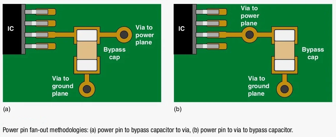
- Power Integrity: Use decoupling capacitors close to power pins to stabilize voltage and reduce noise. For example, a 0.1 μF capacitor placed within 100 mils of a high-speed IC can effectively filter noise.
- Simulation and Testing: Leverage simulation software to model signal behavior before manufacturing. Post-assembly testing with tools like Time-Domain Reflectometry (TDR) can validate impedance and detect issues.
- Thermal Management: Heat can affect dielectric properties and signal performance. Incorporate thermal vias and heat sinks in your HDI design to maintain stable operating conditions.
These additional considerations can make a significant difference in achieving reliable performance in compact HDI assemblies.
Conclusion: Building Reliable HDI Designs with High Signal Integrity
Achieving high signal integrity in HDI assembly is no small feat, but with the right strategies, it’s entirely possible. By focusing on impedance control in HDI, crosstalk reduction in HDI, strategic signal layer placement, and tailored high-frequency HDI design, engineers can create compact, high-performance boards that meet the demands of modern electronics.
Start with a solid foundation—choose the right materials, plan your layer stack-up carefully, and use simulation tools to predict and resolve issues before they arise. Whether you’re designing for consumer gadgets or industrial applications, these principles will help ensure your HDI assembly delivers reliable signal integrity every time.
At ALLPCB, we’re committed to supporting engineers with the tools and expertise needed to bring innovative designs to life. With these tips in hand, you’re well on your way to mastering HDI assembly signal integrity in even the most compact designs.


