 ALLPCB


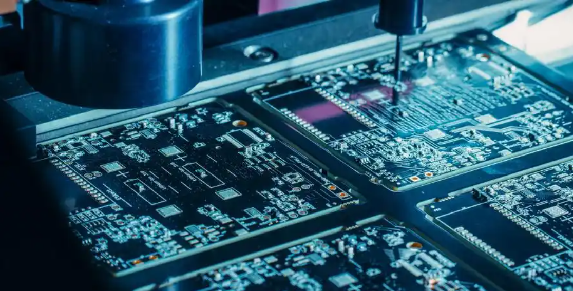
If you're an electrical engineer looking to optimize PCB testing, you might be wondering how to achieve the best test coverage and fault detection. The answer lies in bed-of-nails testing with ICT (In-Circuit Test) fixtures. This method offers unparalleled precision and efficiency for high-volume PCB production by ensuring comprehensive fault detection through direct contact with multiple test points. In this blog, we’ll dive deep into the advantages of ICT fixtures, explore how they maximize test coverage, and compare them to alternatives like flying probe testing. Whether you're troubleshooting complex boards or aiming to streamline production, this guide will equip you with actionable insights.
What Is Bed-of-Nails Testing and Why Does It Matter?
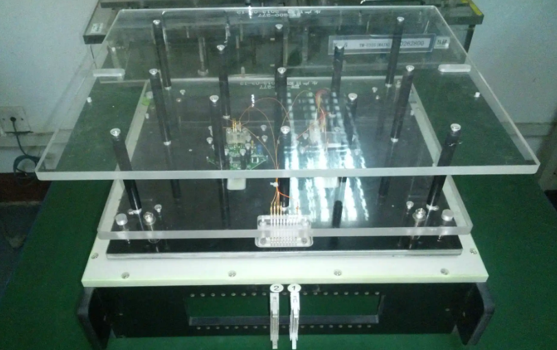
Bed-of-nails testing is a cornerstone of In-Circuit Testing (ICT), a method used to evaluate the functionality of populated printed circuit boards (PCBs). Named for its appearance, a bed-of-nails fixture consists of numerous spring-loaded probes or "nails" that make direct contact with test points on a PCB. These probes check for electrical issues like shorts, opens, and incorrect component values by measuring resistance, capacitance, and other parameters.
For electrical engineers, the importance of bed-of-nails testing lies in its ability to detect faults early in the manufacturing process. By identifying issues at the component level before final assembly, it reduces costly rework and ensures high-quality output. This is especially critical in industries like automotive or aerospace, where a single faulty PCB can lead to catastrophic failures.
Key ICT Fixture Advantages for PCB Testing
ICT fixtures using the bed-of-nails approach bring several benefits to the table. Let’s break down why this method is often the go-to choice for high-volume PCB manufacturing and how it can help engineers achieve reliable results.
1. Superior Test Coverage
One of the standout advantages of bed-of-nails testing is its ability to provide extensive test coverage. Unlike other methods that may only access a limited number of nodes, ICT fixtures can simultaneously contact hundreds or even thousands of test points on a PCB. This means you can test almost every component and connection in a single pass, ensuring no fault goes undetected. For instance, in a complex PCB with 500+ test points, a well-designed ICT fixture can achieve up to 95% test coverage, compared to lower percentages with alternative methods.
2. High-Speed Fault Detection
Speed is crucial in production environments, and ICT fixtures excel here. Once the fixture is set up, testing a single board can take just a few seconds. This is because all probes make contact at once, allowing for parallel testing of multiple circuits. For high-volume runs, this translates to significant time savings. Imagine testing 10,000 boards—ICT can complete this in hours, while slower methods might take days.
3. Precision and Repeatability
Bed-of-nails fixtures are engineered for precision. Each probe is positioned to align perfectly with specific test points on the PCB, ensuring consistent and repeatable results. This is vital for engineers who need reliable data to diagnose issues like a short circuit with a resistance reading below 1 ohm or a capacitance deviation beyond 5%. The repeatability also means that every board in a batch is tested under identical conditions, reducing variability in quality control.
4. Cost-Effectiveness for High Volumes
While the upfront cost of designing and building an ICT fixture can be high—often ranging from $10,000 to $50,000 depending on complexity—the long-term savings are substantial for large production runs. The per-board testing cost drops significantly as volume increases, making it more economical than alternatives for batches of 1,000 units or more. This is a critical consideration for engineers managing budgets in mass production.
How Bed-of-Nails Testing Enhances PCB Fault Detection
Fault detection is the heart of PCB testing, and bed-of-nails ICT fixtures are uniquely equipped to identify a wide range of issues. Here’s how they excel in this area and why they’re indispensable for engineers.
Detecting Shorts and Opens
Shorts and opens are among the most common PCB defects. A short circuit might occur due to solder bridges, showing a resistance reading near 0 ohms, while an open circuit could result from a broken trace, showing infinite resistance. Bed-of-nails testing can pinpoint these issues by measuring electrical continuity across all test points simultaneously, ensuring no defect slips through.
Component-Level Testing
ICT fixtures go beyond basic connectivity checks. They can measure specific component values like resistor tolerances (e.g., verifying a 10kΩ resistor is within ±1% of its rated value) or capacitor performance (e.g., ensuring a 100nF capacitor operates within expected limits). This granular level of testing helps engineers catch faulty components before they cause systemic failures.
Early Fault Identification
By integrating ICT early in the production process, faults can be identified before additional assembly steps add cost and complexity. For example, detecting a misplaced diode with a forward voltage drop outside the typical 0.7V range during ICT prevents downstream issues in functional testing or field deployment. This early intervention saves time and resources, a priority for any engineering team.
ICT vs Flying Probe: Which Is Better for Your Needs?
When choosing a PCB testing method, engineers often compare bed-of-nails ICT with flying probe testing. Both have their strengths, but understanding their differences is key to selecting the right approach. Let’s break down the comparison across critical factors.
Test Coverage and Accuracy
As mentioned, ICT fixtures with bed-of-nails offer near-complete test coverage, often above 90%, due to their ability to access multiple points at once. Flying probe systems, on the other hand, use movable probes to test points sequentially, which can limit coverage to around 70-80% on complex boards. While flying probes are precise for the points they do test, they can miss issues in densely populated areas due to accessibility constraints.
Speed and Production Volume
Speed is where ICT shines. A bed-of-nails fixture can test a board in under 10 seconds, making it ideal for high-volume production (1,000+ units). Flying probe testers, however, take longer—often 1-2 minutes per board—since probes move one at a time. This makes flying probes better suited for low-volume runs, prototypes, or boards with frequent design changes.
Cost and Setup Time
Upfront costs for ICT fixtures are high due to custom design and manufacturing, but they become cost-effective over large volumes. Flying probe systems have lower initial costs since they don’t require custom fixtures, but per-board testing costs remain higher due to slower speeds. Setup time also differs: ICT fixtures take weeks to design and build, while flying probe systems can be programmed and ready in hours, offering flexibility for rapid prototyping.
Flexibility and Design Changes
Flying probe testing wins in flexibility. Since it uses software-controlled probes, adapting to a new PCB layout is as simple as updating the test program. With ICT fixtures, any design change might require rebuilding the fixture, adding cost and delay. For engineers working on iterative designs, flying probe can be a more practical choice despite its slower speed.
Practical Tips for Implementing Bed-of-Nails ICT Fixtures
For engineers looking to integrate bed-of-nails testing into their workflow, here are some actionable tips to maximize effectiveness and avoid common pitfalls.
Design for Testability (DFT)
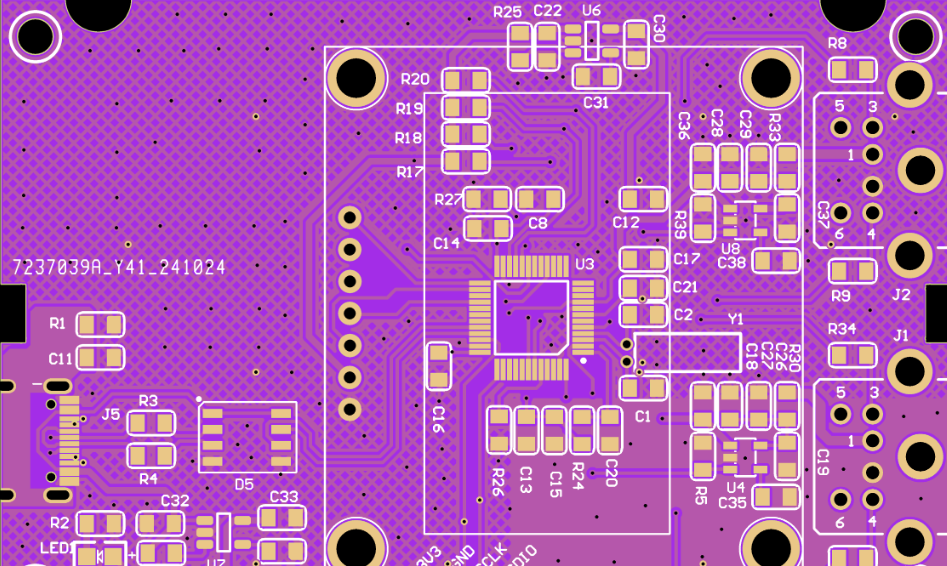
Ensure your PCB layout includes accessible test points for the ICT fixture. Place test pads on a 0.1-inch grid for compatibility with standard fixtures, and avoid placing them under components where probes can’t reach. Collaborating with your test engineer during the design phase can prevent costly redesigns later.
Optimize Fixture Design
Work with your fixture manufacturer to balance cost and coverage. For instance, if full coverage isn’t feasible due to budget constraints, prioritize critical circuits or high-risk areas like power lines with currents exceeding 5A. Also, consider dual-sided fixtures for double-sided boards to access test points on both sides.
Regular Maintenance
Probes in a bed-of-nails fixture can wear out or become contaminated with flux residue, leading to false readings. Schedule regular cleaning and probe replacement—typically after 100,000 cycles—to maintain accuracy. A worn probe might fail to detect a short with a resistance as low as 0.5 ohms, compromising quality.
Challenges and Limitations of Bed-of-Nails ICT
While bed-of-nails testing offers significant advantages, it’s not without challenges. Being aware of these limitations helps engineers make informed decisions.
High Initial Investment
As noted, the cost of custom ICT fixtures can be a barrier, especially for small-scale projects. For a complex board, fixture costs can exceed $30,000, making it less viable for runs under 500 units.
Limited Flexibility
Once built, an ICT fixture is specific to a single PCB design. Any layout change—like moving a test point by just 0.05 inches—can render the fixture obsolete, requiring a new one. This rigidity contrasts with the adaptability of flying probe systems.
Accessibility Issues
On ultra-dense PCBs with fine-pitch components (e.g., 0.4mm pitch BGA packages), fitting probes for every test point becomes challenging. This can reduce test coverage, forcing engineers to rely on alternative methods for certain areas.
Real-World Applications: When to Choose Bed-of-Nails ICT
Bed-of-nails ICT fixtures are best suited for specific scenarios. For example, in automotive electronics manufacturing, where thousands of control unit PCBs are produced daily, ICT ensures each board meets stringent quality standards by detecting faults like a 2% deviation in resistor values. Similarly, in consumer electronics like smartphones, ICT’s speed supports rapid production cycles, testing boards at a rate of one every 5 seconds.
On the other hand, for a startup developing a new IoT device with frequent design iterations, flying probe testing might be more practical during the prototype phase due to its flexibility and lower setup cost. Once the design stabilizes and production scales, transitioning to ICT can maximize efficiency.
Conclusion: Leveraging the Bed-of-Nails Advantage
For electrical engineers, bed-of-nails testing with ICT fixtures offers a powerful solution to maximize test coverage and enhance PCB fault detection. Its ability to test multiple points simultaneously, deliver high-speed results, and provide cost savings in high-volume production makes it a go-to method for many industries. While it has limitations like high upfront costs and limited flexibility, these can often be mitigated with careful planning and design for testability.
Compared to flying probe testing, ICT stands out for large-scale manufacturing, while flying probe suits prototypes and low volumes. By understanding your project’s needs—whether it’s speed, coverage, or adaptability—you can choose the right approach. Have you used bed-of-nails ICT in your projects? Share your experiences or challenges in the comments below—we’d love to hear how it’s worked for you!
Ready to implement ICT fixtures or optimize your PCB testing process? Start by evaluating your production volume and design complexity, and consider consulting with a test equipment specialist to design a fixture tailored to your needs. With the right setup, the bed-of-nails advantage can transform your quality control and ensure flawless PCB performance.


