 ALLPCB


In the world of electronics, Printed Circuit Boards (PCBs) are the backbone of almost every device we use. From smartphones to industrial machinery, PCBs connect components and ensure smooth operation. However, manufacturing these boards comes with challenges, one of the most common being short circuits. These faults can disrupt functionality and lead to costly failures. So, how do manufacturers handle PCBs in production and detect shorts effectively? This blog dives deep into the process of PCB manufacturing with a focus on Surface Mount Technology (SMT) PCB assembly, and explores methods like SEM inspection of joints, soldering techniques, and testing semiconductors to identify and prevent shorts.
At ALLPCB, we understand the importance of quality and precision in electronics manufacturing. In this comprehensive guide, we'll walk you through the critical steps of PCB production and the advanced techniques used to detect and address short circuits, ensuring reliable and high-performing boards for your projects.
What Are PCBs and Why Are They Crucial in Manufacturing?
PCBs are flat boards made of insulating materials like fiberglass, with conductive copper tracks etched onto them. These tracks connect electronic components such as resistors, capacitors, and semiconductors, forming the circuits that power devices. In manufacturing, PCBs are essential because they provide a compact, organized, and reliable way to assemble complex electronics.
The production of PCBs involves multiple stages, from design and fabrication to assembly and testing. Each step requires precision to avoid defects like short circuits, which occur when unintended connections form between conductive paths, often due to excess solder, misaligned components, or manufacturing errors. Shorts can cause overheating, component failure, or complete device malfunction, making their detection a top priority in the manufacturing process.
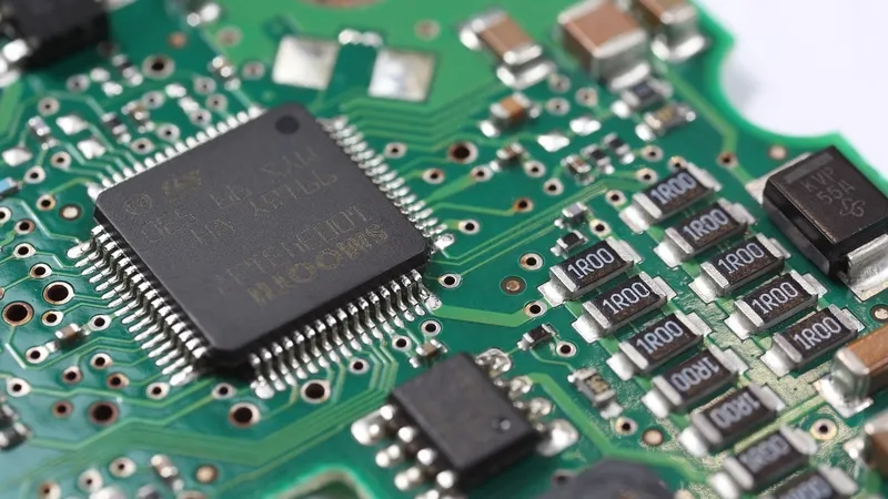
Understanding SMT PCB Assembly in Manufacturing
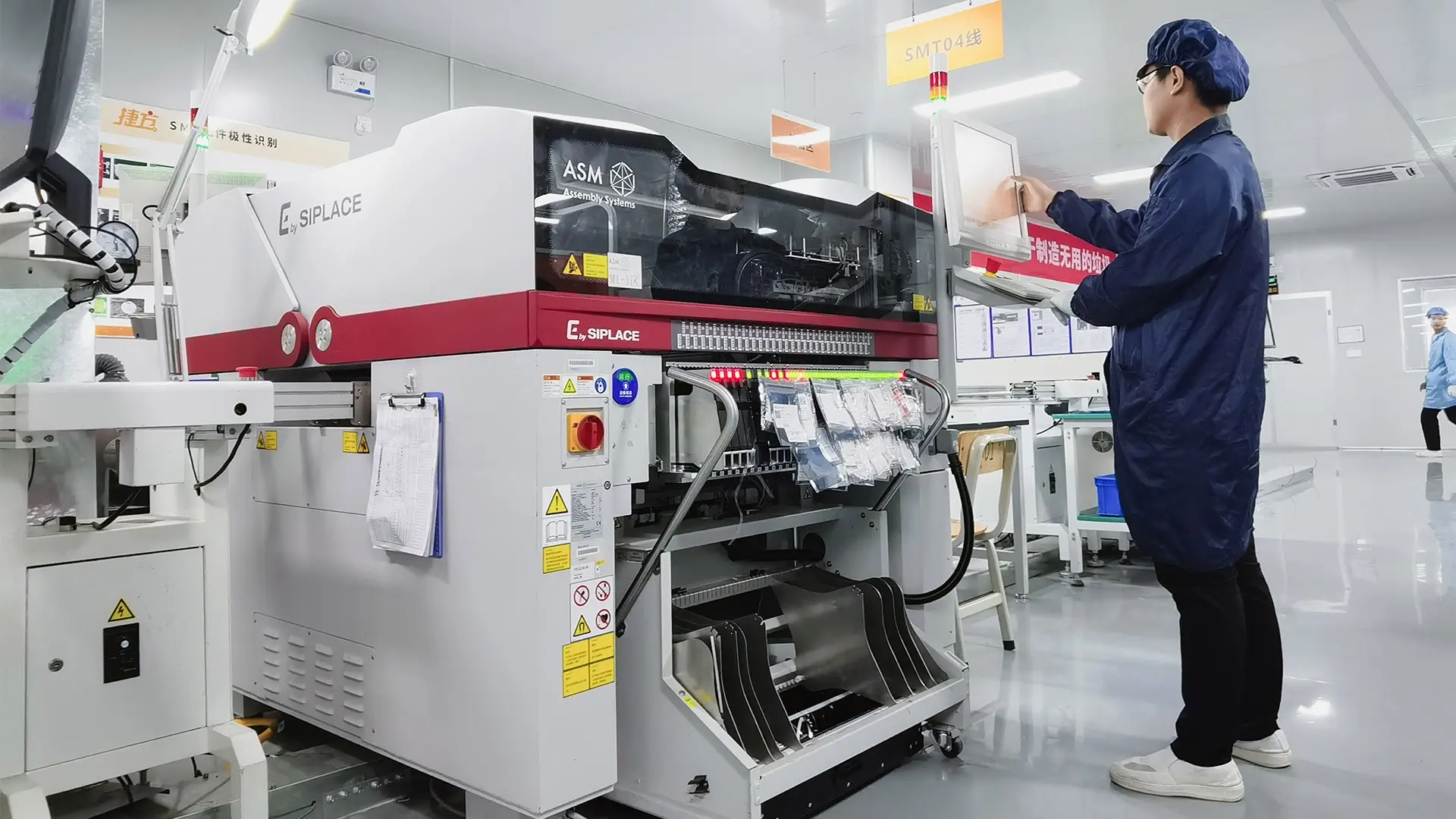
Surface Mount Technology (SMT) is a widely used method in PCB assembly where components are mounted directly onto the surface of the board. Unlike older through-hole techniques, SMT allows for smaller, more densely packed components, making it ideal for modern compact devices. However, the precision required in SMT PCB assembly also increases the risk of defects like shorts.
In SMT assembly, the process begins with applying solder paste to specific areas of the PCB using a stencil. Then, automated machines place components onto the paste with pinpoint accuracy. The board passes through a reflow oven, where the solder paste melts and forms secure connections between the components and the board. While this process is highly efficient, errors such as solder bridging (where solder connects two adjacent pads) or component misalignment can lead to short circuits.
To mitigate these risks, manufacturers rely on strict quality control measures during SMT PCB assembly. For instance, ensuring the solder paste is applied evenly and using high-precision placement machines can reduce the likelihood of defects. Additionally, post-assembly inspection is critical to catch any issues before the boards move to the next stage.
The Role of Soldering in PCB Manufacturing
Soldering is the heart of PCB assembly, as it creates the electrical and mechanical connections between components and the board. In SMT PCB assembly, reflow soldering is the most common technique, where solder paste is heated to a specific temperature (typically around 240-260°C) to form strong bonds. However, poor soldering practices can lead to issues like solder bridges, cold joints, or insufficient solder, all of which can cause short circuits or weak connections.
For example, if too much solder paste is applied, it can overflow during reflow and create unintended connections between adjacent pads, resulting in a short. Similarly, if the reflow oven temperature is not properly controlled, the solder may not melt evenly, leading to defective joints. To prevent these issues, manufacturers often use advanced soldering equipment with precise temperature profiles and monitor the process closely.
Another key aspect of soldering is the choice of materials. Lead-free solder, for instance, is widely used due to environmental regulations, but it requires higher melting temperatures (around 217-220°C) compared to traditional lead-based solder. This can introduce additional challenges in ensuring uniform heating without damaging components. By optimizing soldering parameters and using high-quality materials, manufacturers can significantly reduce the risk of shorts and other defects.
Detecting Shorts in PCBs: Why It Matters
Short circuits are among the most common and damaging defects in PCB manufacturing. They can occur due to various reasons, such as solder bridges, manufacturing debris, or design flaws. A short can cause excessive current flow, leading to overheating (sometimes exceeding safe temperature thresholds of 85°C for many components) or even permanent damage to the board. Detecting and resolving shorts early in the manufacturing process is crucial to avoid costly rework or product failures in the field.
There are several methods to detect shorts, ranging from visual inspections to advanced testing techniques. Each method has its strengths and is often used in combination to ensure comprehensive quality control. Let's explore some of the most effective approaches used in the industry.
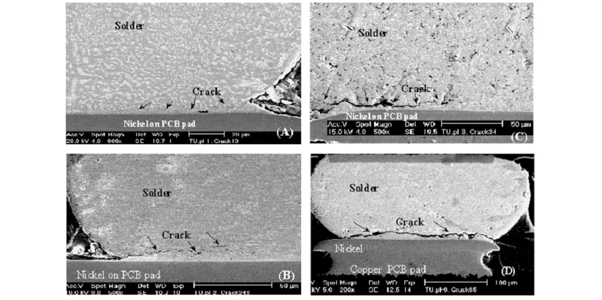
SEM Inspection of Joints for Precision Analysis
Scanning Electron Microscopy (SEM) is a powerful tool used for detailed inspection of solder joints in PCBs. SEM inspection of joints provides high-resolution images (with magnifications up to 100,000x) that reveal microscopic defects invisible to the naked eye or standard optical microscopes. This technique is particularly useful for analyzing the quality of solder joints in SMT PCB assembly, where tiny components and tight spacing make defects harder to detect.
During SEM inspection, a focused beam of electrons scans the surface of the solder joint, producing detailed images of its structure. This allows engineers to identify issues like cracks, voids, or solder bridging that could lead to shorts. For instance, a solder joint with a void percentage above 25% may be considered unreliable, as it can weaken the connection and increase resistance (potentially exceeding 0.1 ohms), leading to overheating.
While SEM inspection of joints is highly accurate, it is typically used for failure analysis or quality assurance in high-stakes applications due to its cost and time requirements. For mass production, manufacturers often combine SEM with other inspection methods to balance efficiency and precision.
Testing Semiconductors and Electrical Performance
Semiconductors, such as diodes, transistors, and integrated circuits, are critical components on a PCB, and their proper functioning is essential for the board's performance. Testing semiconductors during manufacturing helps identify issues like shorts or open circuits that could affect the entire system. This process often involves checking electrical parameters like voltage, current, and resistance to ensure they meet design specifications.
One common method for testing semiconductors is In-Circuit Testing (ICT), which uses a bed of nails tester or flying probe system to measure electrical performance. ICT can detect shorts by applying test signals and checking for unexpected current paths. For example, if a test point shows a resistance value below 1 ohm between two unrelated pins, it may indicate a short circuit. ICT is highly effective for detecting manufacturing defects and ensuring that semiconductors are correctly connected.
Another approach is Functional Circuit Testing (FCT), where the PCB is powered on and tested under real-world operating conditions. This method helps identify shorts that may only manifest during active use, such as those caused by thermal expansion or dynamic current loads. By combining ICT and FCT, manufacturers can achieve a thorough assessment of semiconductor performance and overall board reliability.
Other Inspection Techniques for Detecting Shorts
Beyond SEM inspection and semiconductor testing, several other techniques are widely used to detect shorts in PCB manufacturing. These methods provide varying levels of detail and are often chosen based on the production volume and complexity of the board.
Automated Optical Inspection (AOI)
AOI uses high-resolution cameras and image processing software to visually inspect PCBs for defects. It can quickly identify issues like solder bridges or misaligned components in SMT PCB assembly. While AOI is fast and suitable for high-volume production, it may miss hidden defects under components like Ball Grid Arrays (BGAs).
X-Ray Inspection
X-ray inspection is ideal for examining hidden solder joints, such as those in BGAs. It uses penetrating rays to create images of internal structures, revealing shorts caused by excess solder or poor connections. This method is especially useful for complex, multi-layer boards where visual inspection is insufficient.
Thermal Imaging
Thermal imaging detects shorts by identifying areas of excessive heat on the PCB. When a short circuit occurs, current flows through unintended paths, generating heat (often exceeding 100°C in severe cases). Thermal cameras can pinpoint these hotspots, helping engineers locate and fix the issue before it causes damage.
Preventing Shorts During PCB Manufacturing
While detecting shorts is critical, preventing them in the first place is even better. Manufacturers can take several steps to minimize the risk of shorts during PCB production. First, optimizing the PCB design is key. Ensuring adequate spacing between traces (typically at least 0.2 mm for standard designs) and using design rule checks (DRC) can prevent potential shorting points.
Second, maintaining strict control over the SMT PCB assembly process is essential. This includes using high-quality solder paste, calibrating reflow ovens for precise temperature control (within ±5°C of the target profile), and regularly cleaning equipment to avoid contamination. Additionally, training operators to handle components and boards carefully can reduce human error.
Finally, implementing robust quality assurance processes, such as pre-production testing and regular equipment maintenance, helps catch issues early. By focusing on prevention, manufacturers can save time, reduce costs, and deliver reliable PCBs to their customers.
Why Choose ALLPCB for Your PCB Manufacturing Needs?
At ALLPCB, we prioritize quality and precision in every step of PCB manufacturing. Our advanced SMT PCB assembly lines, state-of-the-art inspection tools, and rigorous testing protocols ensure that your boards are free from defects like shorts. Whether you need detailed SEM inspection of joints, comprehensive semiconductor testing, or optimized soldering processes, we have the expertise and technology to deliver top-notch results.
Our commitment to excellence means you can trust us to handle projects of any complexity, from prototype to mass production. With a focus on customer satisfaction and fast turnaround times, we aim to be your reliable partner in electronics manufacturing.
Conclusion
PCBs are the foundation of modern electronics, and their manufacturing requires meticulous attention to detail to avoid issues like short circuits. Through advanced techniques such as SMT PCB assembly, SEM inspection of joints, precise soldering, and thorough testing of semiconductors, manufacturers can detect and prevent shorts effectively. By combining automated inspections like AOI and X-ray with specialized tools like thermal imaging, the industry ensures that PCBs meet the highest standards of quality and reliability.
Understanding these processes not only helps engineers and manufacturers produce better boards but also ensures that end users receive dependable products. At ALLPCB, we're dedicated to pushing the boundaries of PCB manufacturing, delivering solutions that power innovation. Whether you're working on a small project or a large-scale production run, trust us to provide the expertise and support you need for success.


