ALLPCB


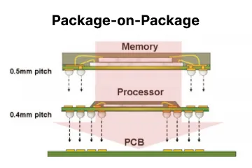
Package-on-Package (PoP) assembly is a special PCB manufacturing method. It stacks two or more semiconductor packages on top of each other. This saves space on the board and boosts the performance of electronic devices.
The two main parts of PoP are usually a logic chip and a memory chip. The logic chip can be a microprocessor or SoC. The memory chip is often DRAM. However, this can change depending on the specific use.
This stacked approach has several benefits. It reduces size, speeds up signal transmission between the stacked parts, and improves overall performance.
PoP assembly is commonly used in mobile devices like smartphones, wearables, and tablets. It is also growing in automotive and IoT applications. In these areas, compactness, speed, and efficiency are crucial.
The Detailed PoP Assembly Process
Step 1: Preparation of PCB
The first step in the PoP assembly process is surface preparation. This involves cleaning the PCB to remove any contaminants that could interfere with the soldering process. Contaminants like dust, oils, and other residues can cause poor solder joints, leading to defects such as cold solder joints or short circuits.
- Cleaning Methods: The most common cleaning methods are ultrasonic cleaning and using a controlled air-jet system. This system blows off dust. Inspectors then examine the PCB for cleanliness using microscopes or automated systems.
- Solder paste application: A technician uses a stencil to apply solder paste to the PCB's designated solder pads. You must apply the paste precisely in the correct amounts to ensure optimal soldering. Too much paste can cause bridging, while too little can result in weak solder joints.
Step 2: Bottom Package Placement
After applying the solder paste, the technician puts the bottom component on the PCB. This component is usually the processor or logic chip. We use high-precision pick-and-place machines to complete this task. This machine uses cameras and vision systems to align the components to the solder pads.
- Alignment: This step requires high accuracy to ensure the IC perfectly aligns with the PCB pads. Misalignment can lead to improper electrical connections, which may cause the device to malfunction.
- Placement Precision: Some PoP designs require components to have a very fine pitch (distance between leads), which increases the precision needed during placement. The pick-and-place machines used here are highly specialized and can align components down to micrometer-level precision.
Step 3: Top Package Placement
The next step is placing the top component, typically a memory IC or additional peripheral IC, on top of the bottom component. These components connect through small solder balls, also known as "ball grid array" (BGA) connections.
- Placement Considerations: During this step, it’s essential to maintain proper alignment with the bottom component to ensure a secure, reliable connection. This is done using a second pick-and-place machine or a dual-gantry system that allows precise stacking.
- Solder Balls: The top package is pre-balled with solder spheres that will melt during reflow soldering to make connections. The size of the balls varies depending on the component pitch, and the solder balls must be uniformly sized to avoid inconsistent soldering.
Step 4: Reflow Soldering
Reflow soldering is a critical step in the PoP assembly process. Both the bottom and top ICs undergo reflow soldering in an oven with a carefully controlled thermal profile. This ensures the solder paste melts and forms a solid, reliable bond between the components and the PCB.
- Thermal Profile: The reflow oven follows a precise temperature curve. The process typically includes four stages: preheat, soak, reflow, and cooling. The temperature must be carefully controlled to avoid overheating the components, which could damage sensitive ICs.
- Multiple Layers: In PoP, the reflow soldering process is unique because both packages (top and bottom) are reflowed simultaneously, which can be challenging as it requires managing heat distribution across stacked components.
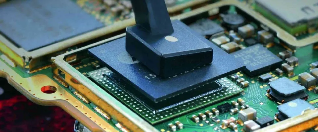
Step 5: Inspection and Testing
Once the components are soldered onto the PCB, the assembly undergoes inspection. This step ensures the quality of the solder joints and verifies that there are no misalignments or defects in the package stacking.
- X-ray Inspection: X-ray inspection is often used to detect hidden defects such as voids in the solder joints, which can be invisible to the naked eye. X-ray machines are able to inspect the joints between the stacked packages, where traditional visual inspections might fail.
- Automated Optical Inspection (AOI): AOI systems use cameras to visually inspect the PCB for surface defects such as misplaced components, broken leads, or insufficient soldering. AOI is an essential tool in the PoP assembly process, as it quickly detects defects that could affect the functionality of the device.
- Electrical Testing: After inspection, the assembled PCB undergoes electrical tests to verify that all components are functioning correctly. This may involve using in-circuit testing (ICT) or functional testing systems to simulate the operational environment of the device.
Benefits of PoP Assembly
1. Space Efficiency
PoP assembly enables manufacturers to fit more components into smaller spaces, which is essential for modern electronics. The vertical stacking of ICs optimizes PCB space, which allows for the miniaturization of devices without sacrificing performance.
2. Improved Signal Integrity
By reducing the distance between components, PoP technology improves signal integrity, particularly for high-speed data transfer between the processor and memory. The reduced distance minimizes the delay in signal transmission, which is crucial for high-performance applications.
3. Cost-Efficiency
PoP reduces the need for multiple separate PCBs or complex interconnects, which can save costs in terms of both materials and assembly time. The combined reflow process also simplifies production compared to traditional multi-board assembly.
4. Design Flexibility
PoP offers flexibility in design because manufacturers can mix and match different chips according to specific needs. This allows for custom configurations tailored to the unique requirements of each product.
Challenges in PoP Assembly and How to Overcome Them
Thermal Management
PoP devices generate more heat because of their compactness and stacked configuration. Effective thermal management solutions, such as thermal vias, heat sinks, and special heat-dissipating materials, are necessary to ensure reliable performance.
- Thermal Vias: A thermal via is a hole filled with a material that allows heat to be conducted from the component to the PCB's surface, where it can be dissipated.
- Heat Sinks: In some cases, heat sinks may be added to the top or bottom of the stacked components to improve heat dissipation.
Precision and Alignment
Misalignment during placement of the stacked packages can lead to defects such as short circuits or poor electrical performance. High-precision equipment is essential to avoid these problems.
Advanced Pick-and-Place Machines
Modern placement machines have advanced vision systems and laser alignment tools. These features ensure the precise placement of components.
Complexity and Cost of Manufacturing
The PoP process needs special equipment, advanced soldering methods, and careful inspection systems. These factors can raise PCB fabrication cost. However, the performance and space-saving benefits often offset these costs.
Conclusion: Why PoP Assembly is Essential for the Future of Electronics
As electronics continue to shrink in size while simultaneously growing in performance, PoP assembly has become an indispensable technology for modern PCB manufacturing. Its ability to stack components efficiently, improve performance, and save space makes it ideal for compact devices like smartphones, wearables, and other IoT applications.
By solving the problems of heat control, alignment accuracy, and manufacturing difficulty, PoP assembly provides a strong and reliable solution for creating advanced electronics. Manufacturers using this technology will be prepared for the growing need. There is a demand for smaller devices. People also want faster and more efficient devices.