 ALLPCB


If you're an electrical engineer looking to speed up your PCB design cycles, FPGA prototyping is a powerful solution. By using an FPGA prototyping board, you can test and validate electronic components and system designs before committing to final hardware. This approach not only reduces errors but also cuts down development time significantly. In this blog, we'll dive deep into how FPGA-based system prototyping transforms PCB design prototyping, enhances electronic component testing, and supports rapid prototyping FPGA workflows. Let's explore the practical benefits, tools, and techniques to help you optimize your design process.
What Is FPGA Prototyping and Why Does It Matter?
FPGA prototyping involves using Field-Programmable Gate Arrays (FPGAs) to simulate and test hardware designs before manufacturing the final PCB or ASIC. Unlike software simulations, which can miss real-world issues, an FPGA prototyping board lets you run your design in a hardware environment that closely mimics the final product. This means you can catch functional errors, test timing constraints, and validate system performance early in the cycle.
Why does this matter for electrical engineers? According to industry data, nearly 50% of PCB re-spins are due to functional logic errors that could have been caught earlier. By integrating FPGA-based system prototyping into your workflow, you can achieve first-pass success rates closer to 70-80%, saving weeks or even months of redesign time. Plus, it allows parallel development of hardware and software, accelerating your time-to-market.
How FPGA Prototyping Speeds Up PCB Design Cycles
In traditional PCB design, engineers often rely on multiple iterations of physical prototypes to test and refine their circuits. Each iteration can take weeks due to fabrication and assembly delays. With PCB design prototyping using FPGAs, you can bypass much of this delay by testing your design digitally on hardware that can be reconfigured in hours, not days.
For instance, consider a design for a high-speed communication system with a target signal rate of 2.5 Gbps. Using an FPGA, you can emulate the critical paths of your PCB layout, test signal integrity, and adjust for impedance mismatches (e.g., targeting 50 ohms for differential pairs) without soldering a single component. Tools like Xilinx Vivado or Intel Quartus let you map your design to the FPGA, run real-time tests, and iterate quickly.
This rapid prototyping FPGA approach also supports early software integration. Firmware developers can start coding and testing on the FPGA prototype while the hardware team finalizes the PCB layout. This parallel workflow can shave off 30-40% of the total development timeline for complex projects.
Key Benefits of FPGA Prototyping for Electronic Component Testing
When it comes to electronic component testing, FPGA prototyping offers unmatched flexibility. Here are some key advantages tailored for electrical engineers:
- Real-World Validation: FPGAs allow you to test components under conditions that mimic the final system. For example, you can simulate a power supply IC's response to load transients of 1A/us and verify stability without risking damage to physical hardware.
- Reconfigurability: Unlike fixed prototypes, an FPGA prototyping board can be reprogrammed to test different configurations. Need to swap out a 12-bit ADC for a 16-bit one in your design? Simply update the FPGA firmware to emulate the change.
- Cost Efficiency: Building physical PCB prototypes for every design iteration can cost thousands of dollars. FPGA prototyping reduces this expense by limiting the number of physical revisions needed.
- Timing Analysis: FPGAs let you measure critical timing parameters, such as setup and hold times (e.g., ensuring a 2 ns margin for a 100 MHz clock), to prevent issues in the final PCB.
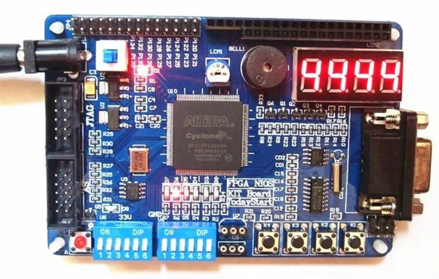
Choosing the Right FPGA Prototyping Board for Your Needs
Not all FPGA boards are created equal, and selecting the right one for FPGA-based system prototyping depends on your project requirements. Here’s what to consider:
- Logic Capacity: Ensure the FPGA has enough logic elements (LEs) or configurable logic blocks (CLBs) for your design. For a mid-range SoC design, a board with 100,000 LEs (like the Xilinx Spartan-7 series) might suffice.
- I/O Capabilities: Check the number and type of I/O pins. If your PCB design involves high-speed interfaces like PCIe (up to 5 Gbps), you’ll need a board with transceivers supporting those speeds.
- Connectivity: Look for boards with USB, Ethernet, or JTAG interfaces for easy debugging and data transfer during PCB design prototyping.
- Software Support: Ensure compatibility with design tools you already use, such as Vivado for Xilinx FPGAs or Quartus for Intel devices.
Popular options include the Digilent Nexys A7 (Xilinx Artix-7 FPGA, ~50,000 LEs, ideal for small to medium projects) and the Terasic DE10-Nano (Intel Cyclone V, with ARM Cortex-A9 for embedded systems). For larger designs, consider high-end boards like the Xilinx Zynq UltraScale+ MPSoC, which supports multi-gigabit transceivers and over 500,000 LEs.
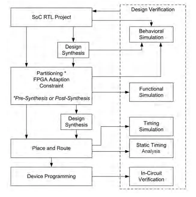
Step-by-Step Guide to FPGA Prototyping in PCB Design
Ready to integrate rapid prototyping FPGA into your workflow? Follow these steps to streamline your PCB design cycle:
1. Define Your Design Requirements
Start by outlining the key specifications of your PCB, such as clock speeds (e.g., 125 MHz system clock), data rates, and power constraints (e.g., 3.3V logic levels). This ensures your FPGA prototype aligns with the final hardware goals.
2. Select an FPGA Prototyping Board
Based on the criteria above, choose a board that matches your design complexity. For a mixed-signal project, ensure the board supports analog interfaces or has breakout pins for external ADCs/DACs.
3. Map Your Design to the FPGA
Use HDL (Hardware Description Language) like VHDL or Verilog to describe your circuit. Then, synthesize and implement it on the FPGA using tools like Xilinx Vivado. Pay attention to timing reports to ensure critical paths meet your design’s constraints (e.g., no violations for a 10 ns period).
4. Test and Validate Components
Run electronic component testing by connecting real or emulated components to the FPGA board. For example, interface a sensor with a 4-20 mA output to verify signal conditioning logic before PCB fabrication.
5. Debug and Iterate
Use built-in debug tools like logic analyzers or JTAG interfaces to monitor signals in real-time. If a timing issue arises (e.g., a 1 ns skew on a data bus), adjust your design in software and re-upload to the FPGA—no soldering required.
6. Transition to Final PCB
Once validated, use the insights from FPGA prototyping to finalize your PCB layout. The reduced error rate means fewer re-spins and a smoother path to production.
Challenges in FPGA Prototyping and How to Overcome Them
While FPGA-based system prototyping offers many benefits, it’s not without challenges. Here are common hurdles and practical solutions:
- Design Mapping Complexity: Translating a PCB design to an FPGA can be tricky due to differences in architecture. Use partitioning tools to split large designs across multiple FPGAs if needed, and leverage vendor-provided libraries for common IP blocks.
- Timing Discrepancies: FPGA timing may not perfectly match the final PCB due to differences in routing delays (e.g., FPGA internal delay of 0.5 ns vs. PCB trace delay of 1 ns). Mitigate this by adding timing margins during simulation and validating critical paths with oscilloscope measurements.
- Resource Limitations: If your design exceeds the FPGA’s capacity, consider offloading non-critical functions to external hardware or upgrading to a higher-capacity board.
Real-World Applications of FPGA Prototyping
FPGA prototyping is widely used across industries for PCB design prototyping. Here are a few examples:
- Automotive Systems: Engineers use FPGAs to prototype ADAS (Advanced Driver Assistance Systems) controllers, testing sensor fusion algorithms at 100 Hz refresh rates before PCB production.
- Telecommunications: High-speed data systems (e.g., 10 Gbps Ethernet) are validated on FPGA boards to ensure signal integrity and jitter performance (e.g., maintaining jitter below 10 ps RMS).
- Consumer Electronics: FPGA prototyping accelerates the design of IoT devices, allowing rapid testing of low-power modes (e.g., 1 mW standby power) and wireless protocols.
Future Trends in FPGA Prototyping for PCB Design
The field of rapid prototyping FPGA is evolving rapidly. Recent articles highlight a growing trend toward modular FPGA platforms that support multi-FPGA setups for massive SoC designs. Additionally, advancements in EDA (Electronic Design Automation) tools are making it easier to map complex designs with millions of gates to FPGAs with minimal manual intervention.
Another exciting development is the integration of AI-driven optimization in FPGA tools. These algorithms can automatically adjust timing constraints or power usage (e.g., reducing dynamic power by 15% through clock gating) during prototyping, further accelerating design cycles.
Conclusion: Why FPGA Prototyping Is a Game-Changer
For electrical engineers, FPGA prototyping is more than just a tool—it’s a game-changer that transforms how we approach PCB design prototyping and electronic component testing. By adopting an FPGA prototyping board in your workflow, you can achieve faster iterations, lower costs, and higher design accuracy through rapid prototyping FPGA techniques. Whether you’re working on a simple microcontroller board or a complex SoC, FPGA-based system prototyping empowers you to test, validate, and refine with confidence.


