ALLPCB


In the world of electronics manufacturing, creating efficient and cost-effective printed circuit boards (PCBs) is crucial. Design for Manufacturability (DFM) in Surface Mount Technology (SMT) offers a strategic approach to streamline production, cut costs, and boost yield. By focusing on DFM principles during the PCB layout and SMT design phases, engineers can avoid common pitfalls, reduce errors, and ensure smoother assembly processes. In this comprehensive guide, we’ll explore how DFM in SMT design and PCB layout can lead to significant cost reduction and improved manufacturing outcomes.
What is Design for Manufacturability (DFM) in SMT?
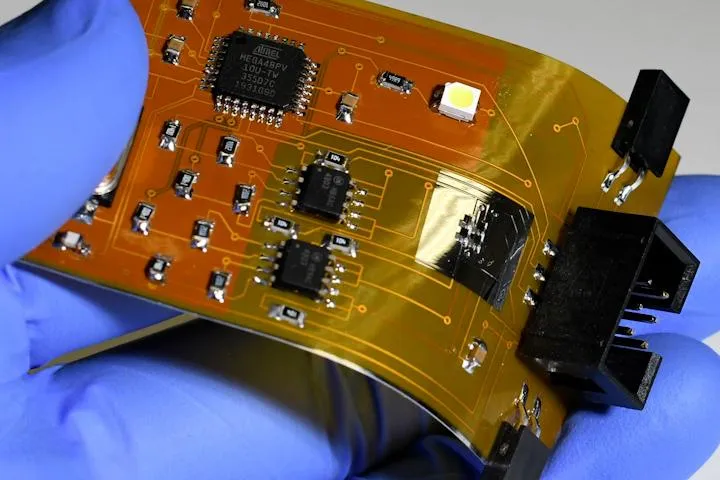
Design for Manufacturability, or DFM, is a set of guidelines and practices aimed at designing products that are easy to manufacture. In the context of SMT, DFM focuses on optimizing PCB layouts for the automated assembly processes used in surface mount technology. SMT involves placing components directly onto the surface of a PCB, and DFM ensures that this process is efficient, error-free, and cost-effective.
By incorporating DFM principles early in the design phase, engineers can minimize manufacturing issues like component misalignment, soldering defects, or assembly delays. This not only reduces production costs but also improves the overall yield—the percentage of usable boards produced in a manufacturing run.
Why DFM Matters for Cost Reduction and Yield Improvement
The primary goal of DFM in SMT design is to bridge the gap between design and production. Without proper DFM practices, manufacturers may encounter challenges such as rework, scrap, or delays, all of which drive up costs. For instance, a poorly designed PCB layout might lead to tombstoning—a defect where one end of a component lifts off the board during soldering—resulting in a failure rate as high as 5-10% in some batches. DFM helps prevent such issues by ensuring designs are compatible with manufacturing capabilities.
Additionally, DFM enhances yield by reducing the likelihood of defects during assembly. Higher yield means more functional boards per production run, directly impacting profitability. Let’s dive deeper into specific DFM strategies for SMT design and PCB layout that can achieve these benefits.
Key DFM Principles for SMT Design
1. Component Placement Optimization
Proper placement of components on a PCB is a cornerstone of DFM in SMT. Components should be arranged to minimize the movement of pick-and-place machines during assembly. Grouping similar components together and aligning them in the same orientation can reduce machine setup time and improve placement accuracy.
For example, placing all resistors in a uniform direction (e.g., with markings facing the same way) can cut down assembly time by up to 15%. Additionally, ensuring adequate spacing between components—typically at least 0.5 mm for small SMT parts like 0402 resistors—prevents soldering defects like bridging, where solder connects adjacent pads unintentionally.
2. Pad and Land Pattern Design
The design of solder pads and land patterns directly affects soldering quality in SMT. DFM guidelines recommend using standard pad sizes as per IPC standards (like IPC-7351) to ensure compatibility with manufacturing equipment. For instance, a typical 0603 resistor pad should measure approximately 0.9 mm x 0.8 mm with a gap of 0.6 mm between pads.
Undersized or oversized pads can lead to issues like insufficient solder or component misalignment. By adhering to recommended dimensions, manufacturers can achieve a soldering defect rate as low as 0.1%, significantly boosting yield.
3. Thermal Management in PCB Layout
Heat dissipation is a critical factor in SMT design. Poor thermal management can cause components to overheat during soldering, leading to failures. DFM practices suggest placing thermal vias—small holes filled with conductive material—under high-power components to transfer heat away from sensitive areas.
For example, a power IC generating 2-3 watts of heat might require 4-6 thermal vias with a diameter of 0.3 mm each to maintain safe operating temperatures. This approach not only improves reliability but also prevents costly rework during production.
DFM Strategies for PCB Layout to Reduce Costs
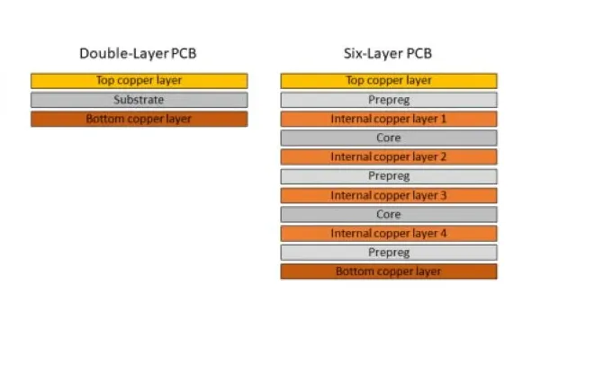
1. Minimize Layer Count
One of the most effective cost reduction strategies in PCB layout is minimizing the number of layers. Each additional layer increases manufacturing complexity and cost—sometimes by 20-30% per layer. For simpler designs, a 2-layer board can often suffice, while more complex projects might require 4-6 layers.
By carefully routing traces and optimizing component placement, engineers can reduce the need for extra layers. This not only cuts material costs but also shortens production time, as fewer layers mean less drilling and lamination steps.
2. Standardize Components and Footprints
Using non-standard or custom components can drive up costs due to special procurement or assembly requirements. DFM encourages the use of widely available, standard components with common footprints. For instance, opting for a standard 0805 capacitor instead of a custom size reduces both component cost and the risk of assembly errors.
Standardization also simplifies inventory management for manufacturers, further lowering overhead costs. A study showed that standardizing components across designs can reduce procurement expenses by up to 10%.
3. Avoid Tight Tolerances Unless Necessary
Designing with overly tight tolerances—such as trace widths below 0.1 mm or drill holes smaller than 0.2 mm—can increase manufacturing difficulty and cost. DFM recommends using tolerances that align with standard fabrication capabilities, like trace widths of 0.15 mm or larger for most applications.
Relaxing tolerances where possible can reduce production costs by 5-15% while maintaining functionality. It also lowers the risk of defects, as standard equipment can handle these specifications more reliably.
Common SMT Design Mistakes to Avoid
1. Insufficient Clearance for Automated Assembly
Automated SMT assembly equipment, like pick-and-place machines, requires adequate clearance around components to operate efficiently. A common mistake is placing components too close to the board edge or to each other, which can lead to machine errors or damage. DFM guidelines suggest a minimum clearance of 3 mm from the board edge and at least 0.5 mm between components.
Ignoring these clearances can result in a rejection rate of up to 8% during assembly, directly impacting yield and increasing costs.
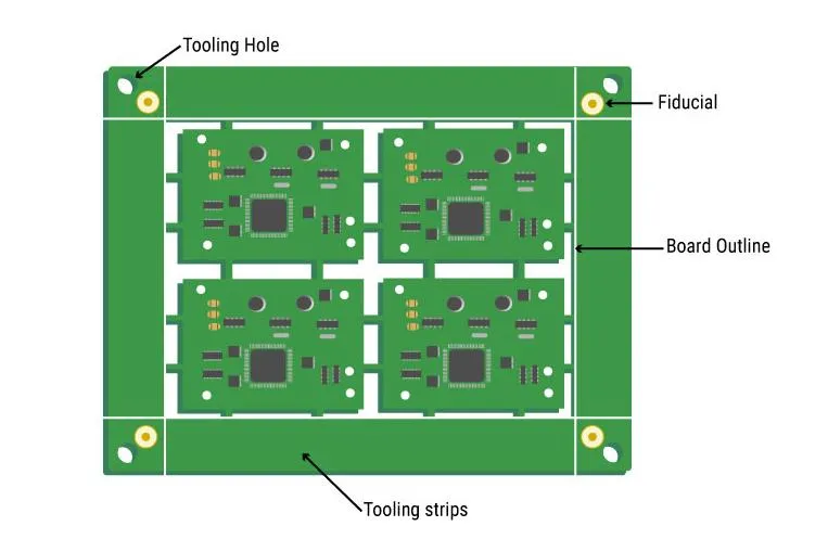
2. Ignoring Panelization for Production
Panelization—the process of grouping multiple PCBs on a single panel for manufacturing—is often overlooked in design. Without proper panel design, manufacturers may waste material or face alignment issues during assembly. DFM advises including fiducial marks (reference points) and breakaway tabs in the layout to ensure precise panelization.
Effective panelization can improve material utilization by 10-20%, reducing waste and lowering overall production costs.
Tools and Technologies Supporting DFM in SMT
Modern design software plays a vital role in implementing DFM principles. Many tools offer built-in DFM checks that analyze PCB layouts for potential manufacturing issues, such as insufficient spacing or non-standard pad sizes. These tools can flag errors before production, saving time and money.
For instance, running a DFM analysis during the design phase can identify up to 90% of potential assembly issues, allowing engineers to make corrections early. Leveraging such technologies ensures that designs are optimized for SMT processes from the start.
Benefits of Implementing DFM in SMT Design
1. Significant Cost Savings
By following DFM guidelines, companies can achieve substantial cost reductions. For example, optimizing component placement and minimizing layer count can lower production costs by 10-25%. Additionally, reducing defects through proper pad design and thermal management cuts down on rework expenses, which can account for 5-15% of total manufacturing costs in poorly designed projects.
2. Higher Manufacturing Yield
DFM directly improves yield by reducing the chances of defects during SMT assembly. A well-designed PCB layout adhering to DFM standards can achieve yields as high as 98-99%, compared to 85-90% for designs with minimal DFM consideration. Higher yield translates to more usable products and better profitability.
3. Faster Time-to-Market
DFM streamlines the transition from design to production by minimizing revisions and manufacturing delays. Designs that are ready for assembly from the outset can shorten lead times by weeks, helping companies bring products to market faster.
Practical Tips for Engineers to Adopt DFM
Start by collaborating with your manufacturing team during the design phase. Understanding their capabilities and limitations—such as minimum trace widths or soldering equipment specs—can guide your layout decisions. Additionally, always run DFM checks using design software to catch issues early.
Another tip is to maintain a library of standard components and footprints for reuse across projects. This practice not only saves design time but also ensures consistency and compatibility with manufacturing processes.
Conclusion: Embrace DFM for Better SMT Outcomes
Design for Manufacturability (DFM) in SMT is a powerful approach to reducing costs and improving yield in PCB production. By optimizing component placement, adhering to standard pad designs, minimizing layer counts, and avoiding common design mistakes, engineers can create layouts that are both efficient to manufacture and reliable in performance. The result is lower production costs, higher yields, and faster time-to-market—all critical factors in today’s competitive electronics industry.
Implementing DFM principles doesn’t require a complete overhaul of your design process. Small, strategic changes in PCB layout and SMT design can yield significant benefits. Start integrating DFM into your workflow today to unlock cost savings and manufacturing success.