 ALLPCB


In the world of PCB assembly and SMT assembly, achieving precise solder paste deposition is critical for high-quality results. Advanced stencil aperture designs play a key role in optimizing this process, ensuring consistent solder paste application and minimizing defects. If you're looking to improve stencil printing outcomes, understanding how aperture design impacts solder paste transfer can make all the difference.
In this comprehensive guide, we'll dive deep into the importance of stencil aperture design, explore various techniques for optimization, and provide actionable insights for engineers and manufacturers involved in PCB assembly. Whether you're dealing with fine-pitch components or high-density boards, these strategies will help elevate your SMT assembly process.
What Is Stencil Aperture Design and Why Does It Matter?
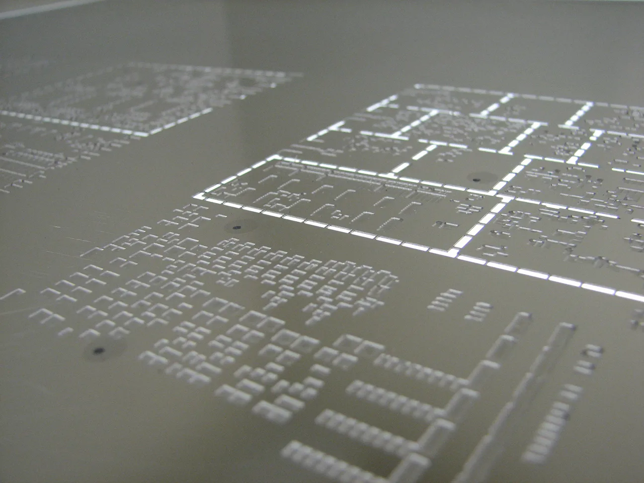
Stencil aperture design refers to the shape, size, and configuration of the openings in a solder paste stencil used during PCB assembly. These apertures dictate how much solder paste is deposited onto the PCB pads, directly affecting the quality of solder joints in SMT assembly. A well-designed aperture ensures the right amount of paste is applied, preventing issues like insufficient solder, bridging, or tombstoning.
In modern electronics manufacturing, where components are shrinking and board designs are becoming more complex, stencil printing has become a critical step. Poor aperture design can lead to inconsistent paste deposition, resulting in costly rework or product failures. By focusing on advanced aperture designs, manufacturers can achieve better control over solder paste volume, improve first-pass yield, and reduce defects.
The Basics of Solder Paste Deposition in PCB Assembly
Before diving into advanced designs, let’s cover the fundamentals of solder paste deposition. During stencil printing, a squeegee pushes solder paste through the stencil’s apertures onto the PCB’s pads. The goal is to deposit a uniform layer of paste that matches the pad size and shape, ensuring proper component placement and soldering.
Key factors influencing solder paste deposition include:
- Stencil Thickness: Thicker stencils deposit more paste, while thinner ones are better for fine-pitch components.
- Aperture Size: The dimensions of the aperture relative to the pad size, often expressed as the area ratio, impact paste release.
- Aperture Shape: Different shapes can improve paste transfer for specific pad geometries.
- Material and Manufacturing: High-precision laser-cut stencils ensure cleaner edges and better paste release.
Optimizing these factors through advanced aperture design can significantly enhance the stencil printing process, especially for challenging applications like high-density interconnect (HDI) boards.
Key Challenges in Solder Paste Deposition
Even with the best equipment, stencil printing can face several challenges that affect solder paste deposition:
- Fine-Pitch Components: As components get smaller (e.g., 0201 or 01005 packages), apertures must be tiny, making paste release harder.
- High-Density Designs: Closely spaced pads increase the risk of solder bridging if too much paste is deposited.
- Paste Release Issues: Poor aperture design can cause paste to stick to the stencil walls, leading to insufficient deposition.
- Stencil Wear: Over time, stencil edges degrade, affecting the consistency of paste application.
Advanced stencil aperture designs address these challenges by tailoring the aperture geometry and dimensions to specific component and board requirements.
Advanced Stencil Aperture Design Techniques
Let’s explore some cutting-edge approaches to stencil aperture design that can optimize solder paste deposition in SMT assembly.
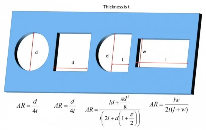
1. Area Ratio Optimization
The area ratio is a critical parameter in stencil design, defined as the ratio of the aperture’s opening area to the area of its walls. A higher area ratio (typically above 0.66) ensures better paste release. For fine-pitch components, reducing stencil thickness or adjusting aperture width can improve this ratio.
For example, a 0.1 mm thick stencil with a 0.2 mm wide aperture has an area ratio of 0.5, which may lead to poor paste release. Increasing the aperture width to 0.3 mm raises the area ratio to 0.75, significantly improving deposition.
2. Aperture Shape Modification
Traditional rectangular or square apertures may not always be ideal for complex pad shapes. Advanced designs use modified shapes like trapezoidal or rounded-corner apertures to enhance paste release and uniformity.
- Trapezoidal Apertures: These have a wider top opening, reducing paste adhesion to stencil walls.
- Rounded Corners: Smooth edges prevent paste buildup in sharp corners, improving deposition consistency.
These modifications are particularly useful for BGA (Ball Grid Array) and QFN (Quad Flat No-Lead) components, where precise paste volume is critical.
3. Step Stencils for Mixed Assemblies
In boards with mixed component sizes, a single stencil thickness may not suffice. Step stencils feature varying thicknesses across different areas, allowing more paste for larger components and less for fine-pitch ones. For instance, a step stencil might have a 0.15 mm thickness for standard components and a 0.1 mm thickness for micro-components, optimizing paste volume across the board.
This design reduces the risk of over- or under-deposition, ensuring reliable solder joints for diverse assemblies.
4. Nano-Coatings for Improved Release
While not strictly an aperture design, applying nano-coatings to stencil surfaces complements advanced designs by reducing paste adhesion. These coatings create a smoother surface, allowing paste to release more easily from small apertures. This is especially beneficial for ultra-fine-pitch components where even minor paste sticking can cause defects.
Benefits of Optimized Stencil Aperture Designs
Investing in advanced stencil aperture designs offers several advantages for PCB assembly and SMT assembly processes:
- Higher Yield Rates: Consistent solder paste deposition reduces defects, improving first-pass yield.
- Reduced Rework Costs: Fewer soldering issues mean less time and money spent on rework.
- Better Performance for Miniaturized Components: Optimized designs support the trend toward smaller, denser electronics.
- Enhanced Product Reliability: Proper solder joints ensure long-term durability and functionality of electronic devices.
Best Practices for Implementing Advanced Aperture Designs
To make the most of advanced stencil aperture designs, consider these practical tips during the design and manufacturing stages of PCB assembly:
1. Collaborate with Design Engineers
Work closely with PCB designers to align stencil aperture designs with pad layouts and component specifications. Early collaboration ensures apertures match the board’s requirements, avoiding costly revisions later.
2. Use Simulation Tools
Leverage software tools to simulate solder paste deposition based on different aperture designs. These tools can predict paste release behavior and help identify the best design before manufacturing the stencil.
3. Test with Sample Runs
Before full-scale production, conduct small test runs with different aperture designs. Measure paste volume and inspect solder joints to determine which design performs best for your specific application.
4. Choose High-Precision Manufacturing
Opt for laser-cut stencils with tight tolerances to ensure accurate aperture dimensions. High-precision manufacturing minimizes variations that could affect paste deposition.
5. Regular Maintenance and Inspection
Inspect stencils regularly for wear and tear, especially around small apertures. Clean stencils after each use to prevent paste buildup, which can distort deposition over time.
Real-World Applications of Advanced Aperture Designs
Advanced stencil aperture designs are making a significant impact across various industries. For instance, in the automotive sector, where reliability is paramount, optimized stencil printing ensures robust solder joints for critical control units. In consumer electronics, these designs enable the assembly of compact devices with ultra-fine-pitch components, meeting the demand for smaller, more powerful gadgets.
In one case, a manufacturer of IoT devices reduced defect rates by 15% after implementing trapezoidal apertures and step stencils for their high-density boards. This improvement not only saved costs but also enhanced product reliability in the field.
Future Trends in Stencil Aperture Design
As electronics continue to evolve, stencil aperture design will keep advancing to meet new challenges. Some emerging trends include:
- 3D-Printed Stencils: Additive manufacturing may allow for highly customized aperture shapes and multi-level stencils.
- AI-Driven Design: Machine learning algorithms could analyze past assembly data to recommend optimal aperture configurations.
- Ultra-Thin Stencils: As components shrink further, stencils with thicknesses below 0.08 mm may become standard for fine-pitch applications.
Staying ahead of these trends will be crucial for manufacturers aiming to maintain a competitive edge in SMT assembly.

Conclusion
Advanced stencil aperture designs are a game-changer for optimizing solder paste deposition in PCB assembly and SMT assembly. By focusing on area ratio optimization, shape modification, step stencils, and other innovative techniques, manufacturers can overcome the challenges of modern electronics assembly. The result is higher yield, lower costs, and better product reliability—key factors for success in today’s competitive market.
Whether you’re working on high-density boards or miniaturized components, investing in stencil aperture design can elevate your stencil printing process. With the right approach and tools, you can achieve consistent, high-quality solder paste deposition that meets the demands of even the most complex projects.
At ALLPCB, we’re committed to supporting engineers and manufacturers with cutting-edge solutions for PCB assembly. Explore our resources and services to take your SMT assembly to the next level.


