 ALLPCB


In the fast-paced world of electronics manufacturing, ensuring the quality and reliability of printed circuit boards (PCBs) is paramount. The IPC-A-600 standard, known as the 'Acceptability of Printed Boards,' serves as the cornerstone for defining quality criteria for PCBs. Developed by the Association Connecting Electronics Industries (IPC), this standard provides visual and dimensional guidelines to ensure PCBs meet the rigorous demands of modern applications, from consumer electronics to aerospace systems. In this blog, we dive deep into the IPC-A-600 standard, exploring its classes, criteria, and practical implications for engineers, while offering actionable insights to enhance your PCB projects.
Whether you're designing a high-speed PCB for 5G applications or a robust board for medical devices, understanding IPC-A-600 is essential for aligning with industry expectations and delivering reliable products. Let's explore what makes this standard a critical tool for engineers and manufacturers alike.
Suggested Reading: IPC Standards Demystified: A Guide to PCB Quality and Reliability
What is the IPC-A-600 Standard?
The IPC-A-600 standard is a globally recognized document that outlines the acceptability criteria for bare printed circuit boards. It provides detailed visual and dimensional guidelines for assessing PCB quality, covering both external and internal features. Unlike IPC-6012, which focuses on performance and manufacturing specifications, IPC-A-600 emphasizes visual inspection, making it an essential reference for inspectors, manufacturers, and designers. The standard is regularly updated, with the latest revision, IPC-A-600K (July 2020), incorporating advancements like microvia technology and flexible PCBs.
The standard categorizes PCB quality into three classes based on their intended use, ensuring that boards meet the specific reliability and performance needs of their applications. By adhering to IPC-A-600, manufacturers can reduce defects, streamline communication with suppliers, and ensure compliance with customer requirements.
The Three IPC-A-600 Classes
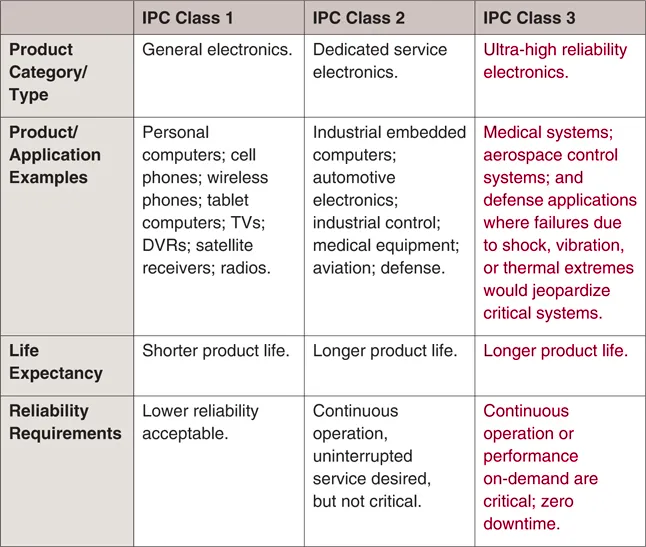
IPC-A-600 defines three classes of PCBs, each with distinct acceptability criteria based on the end-use application. Understanding these classes is crucial for selecting the appropriate quality level for your project.
Class 1: General Electronic Products
Class 1 PCBs are designed for applications where basic functionality is the primary requirement, and extended reliability is not critical. Examples include consumer electronics like toys, low-cost gadgets, or household appliances. The acceptability criteria for Class 1 are the least stringent, allowing for minor imperfections, such as slight solder bridging or small surface scratches, as long as they do not impair function.
- Key Criteria: Minimum annular ring of 0.009 inches (0.23 mm), relaxed tolerances for conductor spacing, and acceptable minor cosmetic defects.
- Applications: LED lights, budget smartphones, or simple remote controls.
Class 2: Dedicated Service Electronic Products
Class 2 PCBs are intended for products requiring extended life and reliable performance, but where uninterrupted operation is not critical. These boards are common in industrial controls, telecommunications equipment, and automotive systems. The criteria are stricter than Class 1, with tighter tolerances for features like plating thickness and conductor width.
- Key Criteria: Minimum annular ring of 0.006 inches (0.15 mm), stricter solder resist coverage, and reduced tolerance for voids or cracks.
- Applications: Networking routers, automotive dashboards, or industrial sensors.
Class 3: High-Performance Electronic Products
Class 3 PCBs are built for critical applications where continuous performance and reliability are non-negotiable, such as aerospace, medical devices, and military systems. These boards undergo the most rigorous inspection, with minimal tolerance for defects like plating voids or dielectric issues.
- Key Criteria: Minimum annular ring of 0.002 inches (0.05 mm), precise conductor spacing (e.g., 0.1 mm for high-density interconnects), and zero tolerance for functional defects.
- Applications: Pacemakers, satellite systems, or avionics control units.
Key Acceptability Criteria in IPC-A-600
The IPC-A-600 standard covers a wide range of criteria for evaluating PCB quality. Below, we highlight the most critical aspects engineers should focus on during inspection.
External Observable Conditions
External features, such as conductor patterns, solder resist, and surface finishes, are evaluated for visual and dimensional compliance. For example:
- Conductor Width and Spacing: Class 3 PCBs require a minimum conductor spacing of 0.1 mm to prevent signal interference in high-speed circuits (e.g., 5G applications with signal speeds exceeding 10 Gbps).
- Solder Resist Coverage: Misalignment of solder resist must not expose more than 0.05 mm of adjacent conductors in Class 3 boards.
- Surface Finish: Common finishes like ENIG (Electroless Nickel Immersion Gold) must have a nickel thickness of 3-6 µm and gold thickness of 0.05-0.2 µm to ensure reliability.
Internal Observable Conditions
Internal features, such as plating thickness and dielectric integrity, require microsection analysis. Key criteria include:
- Plated-Through Hole (PTH) Quality: Class 3 boards require a minimum copper plating thickness of 25 µm in PTHs to ensure robust electrical connectivity.
- Dielectric Separation: Layer-to-layer spacing must be at least 0.08 mm to prevent short circuits in multilayer boards.
- Microvia Integrity: For high-density interconnects (HDI), microvias must have no voids exceeding 10% of the via diameter.
Common Defects and Their Impact
Defects like solder bridging, measling, or delamination can compromise PCB performance. For instance, solder bridging in Class 3 boards can cause signal crosstalk, reducing signal integrity in high-frequency circuits (e.g., 2.4 GHz Wi-Fi modules). IPC-A-600 provides detailed illustrations to classify defects as acceptable, nonconforming, or requiring rework.
Why IPC-A-600 Matters for Engineers
Adhering to IPC-A-600 offers several benefits for engineers and manufacturers:
- Consistency and Communication: The standard provides a universal language for discussing PCB quality, reducing disputes between manufacturers and customers.
- Cost Efficiency: By identifying defects early, manufacturers can avoid costly rework or scrapped boards. For example, detecting a nonconforming annular ring (e.g., 0.001 inches below spec) during inspection prevents component mounting failures.
- Regulatory Compliance: Class 3 PCBs often align with standards like FDA Quality Systems for medical devices or MIL-PRF-31032 for military applications.
- Innovation Enablement: Updates in IPC-A-600K, such as criteria for microvias and flexible PCBs, support cutting-edge technologies like wearable devices and IoT modules.
For engineers, mastering IPC-A-600 ensures that designs meet customer expectations and perform reliably in real-world conditions, whether operating at 1 MHz or 10 GHz.
Practical Tips for Applying IPC-A-600
To effectively implement IPC-A-600 in your PCB projects, consider the following tips:
1. Select the Right Class Early: Determine the PCB class during the design phase to align with application requirements. For example, a Class 3 board for a satellite system requires tighter tolerances (e.g., 0.05 mm conductor spacing) than a Class 1 board for a toy.
2. Invest in Training: IPC-A-600 certification programs, such as the Certified IPC Specialist (CIS), equip inspectors with the skills to identify defects like crazing or plating voids.
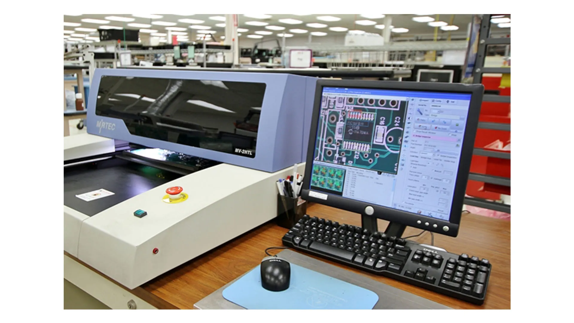
3. Use Automated Inspection Tools: Automated Optical Inspection (AOI) systems can measure conductor widths with 0.01 mm precision, ensuring compliance with IPC-A-600 criteria.
4. Collaborate with Manufacturers: Work closely with your PCB supplier to define acceptability criteria, especially for custom requirements like impedance control (e.g., 50 ohms ± 10% for RF circuits).
5. Document Inspections: Maintain detailed records of inspection results, including defect types and measurements, to trace issues back to manufacturing processes.
How ALLPCB Supports IPC-A-600 Compliance
At ALLPCB, we understand the importance of delivering PCBs that meet the stringent requirements of IPC-A-600. Our advanced manufacturing facilities and quick-turn prototyping services ensure that engineers can achieve Class 1, Class 2, or Class 3 quality with precision. With global logistics and real-time production tracking, we streamline the process from design to delivery, supporting high-reliability applications like medical devices and 5G infrastructure. Our team of experts collaborates with you to verify critical parameters, such as impedance values (e.g., 100 ohms for differential pairs) or microvia integrity, ensuring your boards comply with IPC-A-600 standards and perform flawlessly in the field.
Conclusion
The IPC-A-600 standard is more than just a set of guidelines—it's a blueprint for achieving excellence in PCB manufacturing. By understanding its classes, criteria, and practical applications, engineers can design and inspect boards that meet the demands of today's high-performance electronics. Whether you're working on a Class 1 consumer gadget or a Class 3 avionics system, IPC-A-600 empowers you to deliver quality, reliability, and innovation. At ALLPCB, we're committed to helping you navigate these standards with precision and efficiency, ensuring your projects succeed in a competitive market.
Start applying IPC-A-600 to your next PCB project, and partner with a manufacturer that prioritizes quality at every step. Your designs deserve nothing less.





