 ALLPCB


In the printed circuit board manufacturing process, surface finishing plays a critical role in ensuring the reliability, solderability, and longevity of the board. Two commonly used surface finishing techniques are Hot Air Solder Leveling (HASL) Lead-Free and Electroless Nickel Immersion Gold (ENIG). While both methods serve the purpose of protecting copper traces and facilitating soldering, they differ significantly in their processes, properties, and applications. This article explores what HASL Lead-Free and ENIG are, their key differences, and their respective strengths and weaknesses.
What is HASL Lead-Free?
HASL Lead-Free is a surface finish process where a layer of solder is applied to the PCB surface to create a conductive surface for component soldering. In the case of lead-free HASL, the solder used is typically a mixture of tin and silver or other lead-free alloys, which makes it compliant with modern environmental regulations, like RoHS.
How Does HASL Lead-Free Work?
The HASL PCB is first coated with a thin layer of solder.
The board is then passed through a hot air knife that removes excess solder, leaving a uniform layer of solder on the pads.
The surface is leveled, and the soldered pads are ready for component attachment.
What is ENIG?
ENIG is a more advanced and precise surface finish compared to HASL. ENIG involves a two-step process:
Nickel Layer: A thin layer of nickel(typically 3-6 µm thick) is plated onto the PCB surface through an electroless plating process.
Gold Layer: A thin layer of gold(usually 0.05-0.2 µm) is then applied over the nickel through an immersion process.
This combination of nickel and gold creates a highly durable and corrosion-resistant surface that is widely used for high-performance applications.
Suggested Reading:Selective ENIG Plating Process Guide
Differences Between HASL Lead-Free and ENIG
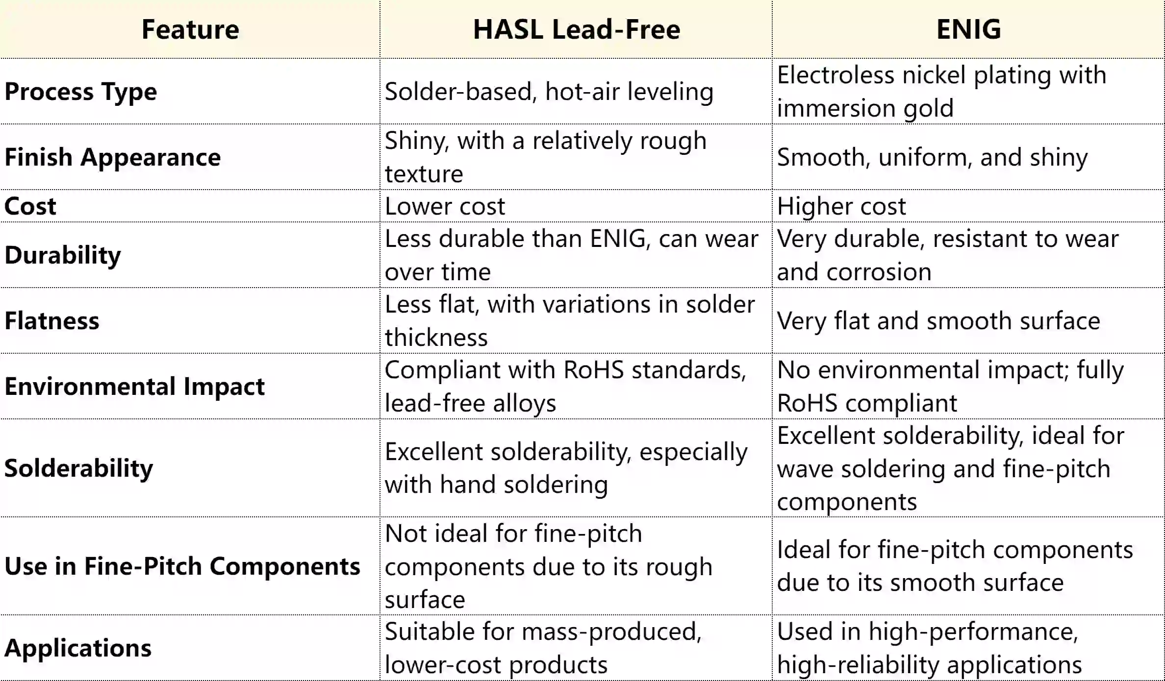
Pros and Cons of HASL Lead-Free
Advantages
Cost-Effective: HASL Lead-Free is one of the most economical surface finishing options, making it ideal for budget-sensitive projects.
Excellent Solderability: The solder coating ensures strong and reliable solder joints.
Widely Available: It’s a well-established process supported by most PCB manufacturers.
Reworkability: Boards with HASL can be easily reworked if needed.
Disadvantages
Uneven Surface: The uneven solder layer can be problematic for fine-pitch or surface-mount components (e.g., BGA or QFN packages).
Thermal Stress: The high temperatures of the molten solder bath can stress the PCB, potentially causing defects in sensitive designs.
Not Ideal for HDI: HASL is less suited for high-density interconnect HDI PCBs due to its lack of precision.
Pros and Cons of ENIG
Advantages
Flat Surface: ENIG’s smooth and uniform finish is perfect for fine-pitch components and advanced assembly techniques.
Corrosion Resistance: The gold layer provides excellent protection against oxidation, enhancing shelf life.
Versatility: Suitable for a wide range of applications, including HDI boards, wire bonding, and mixed assembly (soldering and gold contacts).
Long Shelf Life: ENIG-finished boards can be stored for extended periods without degrading.
Disadvantages
Higher Cost: The use of nickel and gold makes ENIG significantly more expensive than HASL Lead-Free.
Black Pad Risk: Improper process control can lead to “black pad” syndrome, where nickel corrodes, weakening solder joints.
Complex Process: ENIG requires precise chemical management, increasing manufacturing complexity.
Assembly Process
HASL is generally preferred for hand-soldering due to the easy joint formed. If the soldering alloy is close to the HASL’s alloy, adhesion will come very easily and a very strong joint will form as the metals will want to interact on a molecular level. This strong joint also makes HASL a good finish for high-reliability applications.
However, HASL leaves an uneven surface despite the leveling process. ENIG, on the other hand, provides for a very flat surface making ENIG preferable for fine pitch and high pin count components especially ball-grid array (BGA) devices. This flatness allows for accurate placement, controlled amounts of solder, and even heating, thus reducing the risk of opens or shorts due to cold joints or excess solder. In fact, while HASL provides a stronger solder joint, some assemblers have come to prefer ENIG over HASL in all cases because of the flatness.
Conclusion
The decision between HASL and ENIG hinges on your project’s specific needs. HASL’s affordability and high thermal resistance are advantageous for budget-constrained projects or those necessitating multiple reflow processes.
Conversely, ENIG’s flat surface, combined with its RoHS compliance, is well-suited for high-frequency applications, fine-pitch components, and eco-friendly products.
If you need clarification on which surface finish to choose, feel free to reach out to ALLPCB, a leading PCBA fabricator. Our experts can guide you, ensuring you select the right surface finish for a high-yield, cost-effective design that meets your performance expectations.


