ALLPCB


In the world of printed circuit board (PCB) design, a symmetrical stackup is a key factor that directly influences both performance and reliability. But what exactly is a symmetrical stackup, and why does it matter? Simply put, a symmetrical stackup refers to a balanced arrangement of layers in a multilayer PCB, where the layers above and below the center are mirrored in terms of thickness, material, and placement. This design approach significantly enhances symmetrical PCB stackup reliability, improves symmetrical stackup performance impact, and supports critical aspects like symmetrical stackup design for high-speed applications and symmetrical stackup for impedance control.
In this detailed guide, we’ll explore how a symmetrical stackup affects PCB performance and reliability, breaking down its benefits, design considerations, and practical applications. Whether you’re an engineer working on high-speed circuits or a designer aiming for robust boards, this post will provide actionable insights to optimize your designs.
What Is a Symmetrical Stackup in PCB Design?
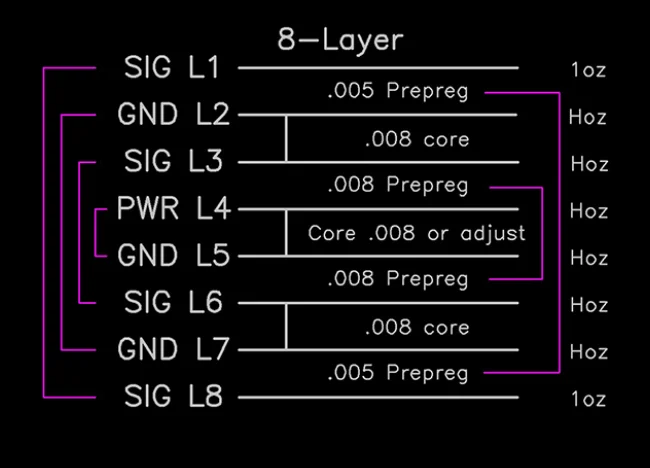
A symmetrical stackup is a method of organizing the layers of a multilayer PCB so that the structure is balanced around its center. For example, in an 8-layer PCB, the top four layers and the bottom four layers would mirror each other in terms of dielectric material, copper thickness, and layer spacing. This balance is not just about aesthetics; it plays a critical role in ensuring the board performs consistently under various conditions.
Without symmetry, a PCB can suffer from uneven stress during manufacturing and operation, leading to issues like warping, signal integrity problems, and even premature failure. By adopting a symmetrical approach, designers can mitigate these risks and create boards that are both reliable and efficient, especially in demanding applications like high-speed data transmission or radio frequency (RF) circuits.
Why Symmetrical Stackup Matters for PCB Reliability
When it comes to symmetrical PCB stackup reliability, the balanced structure offers several advantages that prevent common manufacturing and operational issues. Let’s break down the key reasons why symmetry is essential for a reliable PCB:
- Reduced Warping and Mechanical Stress: During the manufacturing process, PCBs are exposed to high temperatures and pressures. If the stackup is asymmetrical, different layers may expand or contract at uneven rates due to differences in material properties or thickness. This can cause the board to warp or bend, leading to cracks or delamination. A symmetrical stackup ensures uniform thermal expansion, minimizing these risks.
- Improved Durability Under Environmental Stress: In real-world applications, PCBs often face temperature fluctuations, humidity, and mechanical vibrations. A symmetrical design distributes these stresses evenly across the board, reducing the likelihood of failure over time. For instance, in automotive electronics, where boards must withstand harsh conditions, symmetry can extend the lifespan of the product.
- Consistent Manufacturing Outcomes: Manufacturers prefer symmetrical stackups because they are easier to fabricate with predictable results. Asymmetry can lead to uneven pressure during lamination, causing defects like voids or misaligned layers. Symmetry ensures a smoother production process, which translates to fewer rejects and higher reliability.
By prioritizing symmetry, engineers can create PCBs that not only survive the rigors of manufacturing but also perform reliably in the field, even under challenging conditions.
Symmetrical Stackup Performance Impact on High-Speed Designs
The symmetrical stackup performance impact is most evident in high-speed PCB designs, where signal integrity and timing are critical. High-speed applications, such as those involving data rates above 1 Gbps (e.g., USB 3.0, PCIe, or DDR memory), require precise control over signal paths to avoid issues like crosstalk, reflections, and delays. Here’s how a symmetrical stackup contributes to better performance:
- Balanced Signal Propagation: In a symmetrical stackup, the dielectric environment around signal traces on different layers is more consistent. This balance ensures that signals travel at similar speeds across layers, reducing skew in differential pairs. For example, in a high-speed design with a 100-ohm differential impedance requirement, a symmetrical stackup helps maintain this value uniformly, preventing signal mismatch.
- Minimized Crosstalk: Symmetry allows for better placement of ground and power planes, which act as shields between signal layers. By mirroring the layer structure, designers can ensure that high-speed signals are adequately isolated, reducing electromagnetic interference (EMI) and crosstalk. This is especially important in dense designs with multiple high-speed traces.
- Enhanced Power Distribution: A symmetrical stackup often includes paired ground and power planes placed close to each other, creating a low-inductance path for current. This setup improves power integrity by reducing voltage drops and noise, which is crucial for maintaining stable performance in high-speed circuits operating at frequencies above 500 MHz.
Symmetrical Stackup Design for High-Speed Applications
When it comes to symmetrical stackup design for high-speed applications, careful planning is essential to maximize performance. High-speed designs often involve tight timing margins and strict signal integrity requirements, so the stackup must be tailored to meet these needs. Below are key considerations for designing a symmetrical stackup in such scenarios:
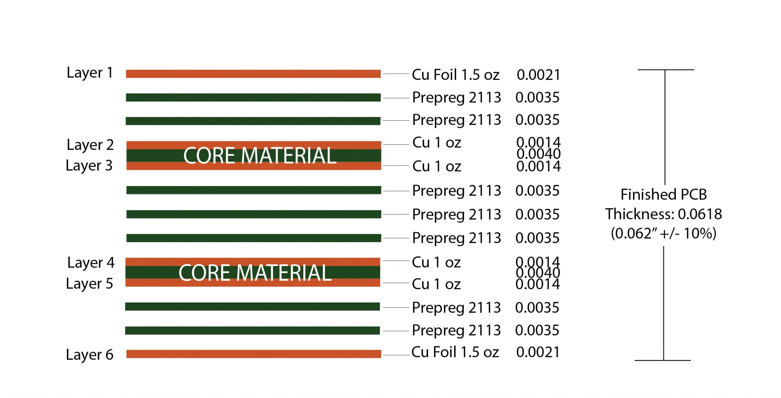
- Layer Count and Arrangement: Choose an even number of layers (e.g., 4, 6, 8) to naturally achieve symmetry. For instance, in a 6-layer board, you might arrange it as Signal-Ground-Power-Power-Ground-Signal. This structure ensures that signal layers are equidistant from reference planes, maintaining consistent impedance.
- Dielectric Material Selection: Use dielectric materials with uniform properties across layers to avoid variations in signal speed. Common materials like FR4 have a dielectric constant (Dk) of around 4.2-4.5, but for high-speed designs, low-loss materials with Dk values closer to 3.0 may be preferred to reduce signal attenuation at frequencies above 1 GHz.
- Trace Routing and Spacing: In a symmetrical stackup, ensure that high-speed traces are routed with equal lengths and consistent spacing on mirrored layers. This practice minimizes skew and maintains signal integrity, especially for differential pairs used in protocols like HDMI or Ethernet.
By adhering to these principles, designers can leverage the benefits of symmetry to create high-speed PCBs that deliver reliable performance, even at data rates exceeding 10 Gbps.
Symmetrical Stackup for Impedance Control
One of the most critical aspects of PCB design is achieving precise impedance control, and a symmetrical stackup for impedance control is a proven strategy to meet this goal. Controlled impedance ensures that signals travel without reflections, which can degrade performance in high-speed and RF applications. Here’s how symmetry supports impedance control:
- Uniform Dielectric Thickness: In a symmetrical stackup, the dielectric layers between signal traces and their reference planes (ground or power) have consistent thickness. This uniformity is crucial for maintaining a target impedance, such as 50 ohms for single-ended traces or 100 ohms for differential pairs. Variations in thickness, common in asymmetrical designs, can cause impedance mismatches.
- Predictable Signal Environment: Symmetry creates a balanced electromagnetic environment around traces, reducing variations in the effective dielectric constant. For example, if a trace on layer 2 is mirrored by a trace on layer 7 in an 8-layer board, both traces experience similar coupling to adjacent planes, ensuring stable impedance values.
- Simplified Design and Simulation: A symmetrical stackup makes it easier to predict and simulate impedance during the design phase. Tools can calculate trace widths and spacing more accurately when the layer structure is balanced, leading to fewer iterations and faster time-to-market.
To achieve optimal impedance control, designers should collaborate closely with their manufacturing partners to confirm material tolerances and layer thicknesses. Even small deviations (e.g., ±10% in dielectric thickness) can affect impedance, so precision in stackup design is paramount.
Practical Tips for Implementing a Symmetrical Stackup
Designing a symmetrical stackup requires attention to detail and an understanding of both design and manufacturing constraints. Below are some practical tips to help engineers implement symmetry effectively:
- Start with an Even Number of Layers: As mentioned earlier, an even number of layers naturally supports symmetry. If an odd number is unavoidable, consider adding a dummy layer to balance the stackup, though this may increase costs.
- Work with Your Manufacturer Early: Share your stackup design with your fabrication partner during the planning stage. They can provide feedback on material availability, tolerances, and potential issues that might affect symmetry during production.
- Use Simulation Tools: Leverage PCB design software to simulate signal integrity, impedance, and thermal behavior of your symmetrical stackup. These tools can identify potential issues before fabrication, saving time and resources.
- Balance Copper Distribution: Ensure that copper density is roughly equal on mirrored layers to avoid uneven heating during soldering or operation. Uneven copper can mimic the effects of an asymmetrical stackup, leading to stress and warping.
By following these guidelines, you can create a symmetrical stackup that enhances both the performance and reliability of your PCB designs.
Challenges and Limitations of Symmetrical Stackups
While symmetrical stackups offer numerous benefits, they are not without challenges. Understanding these limitations can help designers make informed decisions:
- Increased Design Complexity: Achieving perfect symmetry often requires additional planning and coordination, especially in complex designs with mixed-signal requirements. Balancing high-speed and power layers while maintaining symmetry can be tricky.
- Potential Cost Implications: Adding layers or using specific materials to achieve symmetry may increase manufacturing costs. For budget-sensitive projects, designers must weigh the benefits of symmetry against the added expense.
- Space Constraints: In compact designs, adding layers for symmetry might not be feasible due to size limitations. In such cases, designers may need to compromise on symmetry to meet form factor requirements.
Despite these challenges, the advantages of a symmetrical stackup often outweigh the drawbacks, especially for applications where reliability and performance are non-negotiable.
Conclusion: Why Symmetrical Stackup Is a Game-Changer for PCB Design
A symmetrical stackup is more than just a design preference; it’s a strategic choice that can significantly enhance symmetrical PCB stackup reliability and drive a positive symmetrical stackup performance impact. By ensuring balanced thermal expansion, consistent signal propagation, and precise impedance control, symmetry addresses many of the challenges faced in modern PCB design, particularly in symmetrical stackup design for high-speed applications and symmetrical stackup for impedance control.
Whether you’re working on a high-speed data interface, an RF module, or a rugged industrial board, adopting a symmetrical stackup can help you achieve better results with fewer headaches. By carefully planning your layer arrangement, selecting appropriate materials, and collaborating with your manufacturing partner, you can unlock the full potential of this design approach.
At ALLPCB, we’re committed to supporting engineers and designers in creating high-quality, reliable PCBs. A symmetrical stackup is just one of many techniques that can elevate your designs, and we’re here to help you implement it with precision and efficiency.