 ALLPCB


In the fast-paced world of gaming, high-performance consoles demand cutting-edge technology to deliver seamless graphics, rapid processing, and immersive experiences. At the heart of these devices lies a critical component: the printed circuit board (PCB). Specifically, the design and optimization of the PCB stack-up play a vital role in ensuring top-tier performance. For those searching for insights on gaming console PCB stack-up design, PCB layer arrangement for gaming consoles, or related topics like impedance control and material selection, this blog offers a comprehensive guide to mastering the art of layering for maximum efficiency and reliability.
Whether you're an engineer designing the next big console or a tech enthusiast curious about the intricacies of PCB design, this post will walk you through the essentials of creating a high-performance PCB stack-up tailored for gaming applications. Let’s dive into the details of layer arrangement, impedance control, material choices, and high-frequency considerations to ensure your design stands out in the competitive gaming industry.
Why PCB Stack-Up Matters in Gaming Consoles
Gaming consoles are complex systems that handle high-speed data transfer, intricate graphics rendering, and real-time user interactions. The PCB stack-up, which refers to the arrangement of conductive copper layers and insulating materials within the board, directly impacts signal integrity, power distribution, and thermal management. A poorly designed stack-up can lead to issues like signal interference, overheating, or even system failure, all of which are unacceptable in a high-stakes gaming environment.
Optimizing the PCB layer arrangement for gaming consoles ensures that critical components like CPUs, GPUs, and memory modules communicate efficiently. It also minimizes electromagnetic interference (EMI) and maintains stable power delivery, which are essential for consistent performance during intense gaming sessions. With the right stack-up design, engineers can push the boundaries of speed and reliability, delivering consoles that meet the demands of modern gamers.
Key Principles of Gaming Console PCB Stack-Up Design
Designing a PCB stack-up for gaming consoles involves balancing multiple factors, including layer count, material properties, and signal routing. Here are the core principles to keep in mind when approaching gaming console PCB stack-up design.
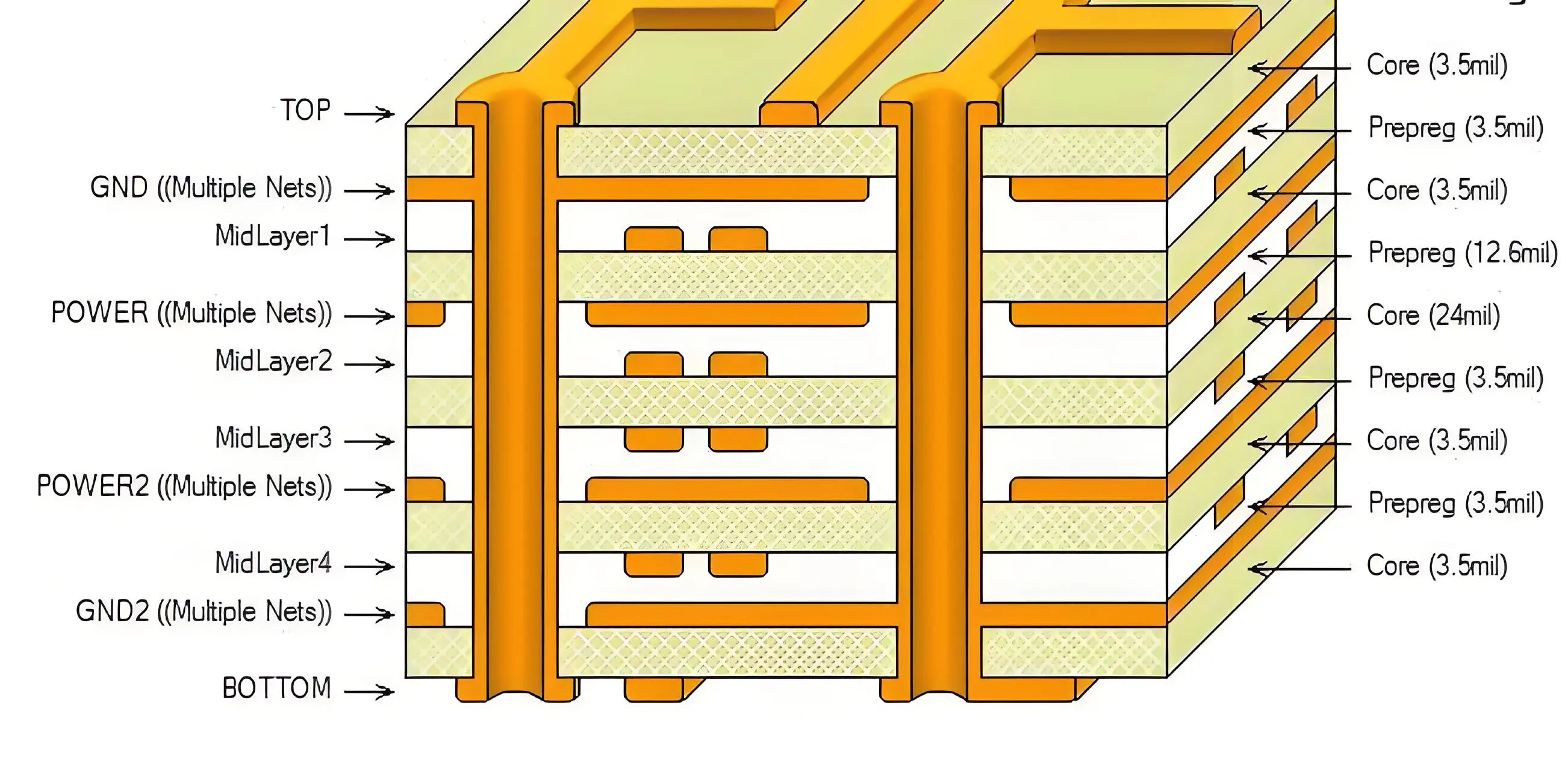
1. Determining the Right Number of Layers
The number of layers in a PCB stack-up depends on the complexity of the gaming console's circuitry. Modern consoles often require 8 to 12 layers or more to accommodate high-speed signals, power distribution, and grounding. For instance, a typical 10-layer stack-up might include:
- Top and bottom signal layers for component connections.
- Multiple internal signal layers for high-speed data lines.
- Dedicated ground and power planes to reduce noise and ensure stable voltage.
More layers allow for better separation of signals and improved EMI shielding, but they also increase manufacturing costs and design complexity. Striking the right balance is crucial for performance and affordability.
2. Layer Arrangement for Signal Integrity
The PCB layer arrangement for gaming consoles must prioritize signal integrity, especially for high-speed signals used in data transfer between processors and memory. A common strategy is to sandwich high-speed signal layers between ground planes. This setup creates a controlled environment for signals, reducing crosstalk and maintaining consistent impedance.
For example, in a 10-layer PCB, you might arrange the layers as follows:
- Layer 1: Top signal (components and routing)
- Layer 2: Ground plane
- Layer 3: High-speed signal
- Layer 4: Ground plane
- Layer 5: Power plane
- Layer 6: Power plane
- Layer 7: Ground plane
- Layer 8: High-speed signal
- Layer 9: Ground plane
- Layer 10: Bottom signal
This arrangement ensures that high-speed signals are shielded by ground planes, minimizing interference and maintaining signal quality.
Impedance Control in PCB Stack-Up for Gaming Consoles
One of the most critical aspects of designing a PCB for high-performance gaming consoles is impedance control in PCB stack-up. Impedance, measured in ohms, refers to the resistance a signal encounters as it travels through a trace. Mismatched impedance can cause signal reflections, leading to data errors and degraded performance.
In gaming consoles, where data transfer rates can exceed 5 Gbps for interfaces like PCIe or DDR memory, maintaining a consistent impedance (often 50 ohms for single-ended signals or 100 ohms for differential pairs) is non-negotiable. Achieving this requires careful stack-up design, including:
- Trace Width and Spacing: Adjusting the width of traces and the spacing between them to match the target impedance.
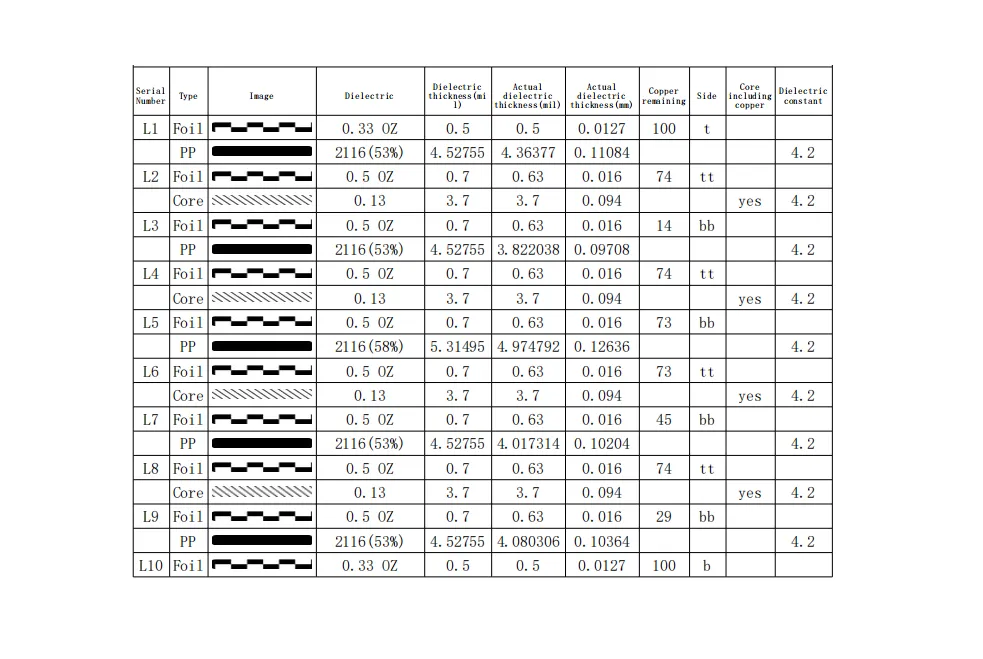
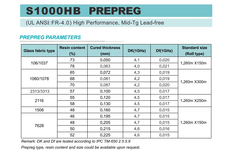
- Dielectric Thickness: Controlling the thickness of the insulating material between layers to influence impedance values.
- Reference Planes: Ensuring signal layers are adjacent to ground or power planes to provide a stable reference for impedance calculations.
Specialized software tools can simulate impedance values during the design phase, allowing engineers to fine-tune the stack-up before manufacturing. For instance, a common dielectric thickness of 0.1 mm between a signal layer and a ground plane can help achieve a 50-ohm impedance for high-speed traces with a width of 0.2 mm.
Choosing the Right Materials for Gaming Console PCBs
The choice of materials in gaming console PCB material selection directly affects the board’s performance, durability, and cost. Gaming consoles operate under high thermal and electrical stress, so selecting materials with the right properties is essential for reliability.
1. Dielectric Materials
The dielectric material, which insulates the copper layers, must have a low dielectric constant (Dk) and low loss tangent (Df) to support high-frequency signals. For gaming consoles handling frequencies above 1 GHz, materials like high-speed laminates with a Dk of around 3.0 to 3.5 and a Df of 0.002 to 0.004 are often preferred over standard FR-4 (Dk of 4.5, Df of 0.02), which may not perform well at higher frequencies.
2. Copper Thickness
Copper thickness impacts current-carrying capacity and signal integrity. For power and ground planes, a thicker copper layer (e.g., 2 oz or 70 μm) ensures stable power delivery, while signal layers may use thinner copper (e.g., 1 oz or 35 μm) to maintain precise impedance control.
3. Thermal Considerations
Gaming consoles generate significant heat during operation, so materials with good thermal conductivity are critical. Some high-performance PCBs incorporate metal cores or thermal vias to dissipate heat effectively, preventing damage to sensitive components.
High-Frequency PCB Stack-Up for Gaming Applications
Modern gaming consoles rely on high-frequency signals for communication between components like GPUs, memory, and storage. Designing a high-frequency PCB stack-up requires extra attention to detail to minimize signal loss and interference.
1. Minimizing Signal Loss
At frequencies above 1 GHz, signal loss due to dielectric absorption and skin effect becomes significant. Using low-loss dielectric materials and ensuring smooth copper surfaces can reduce these losses. Additionally, shorter trace lengths and fewer vias help maintain signal strength.
2. Controlling EMI
Electromagnetic interference can disrupt high-frequency signals, leading to glitches or reduced performance in gaming consoles. A well-designed stack-up with dedicated ground planes and proper layer spacing can shield sensitive signals from external and internal noise sources.
3. Differential Pair Routing
High-frequency interfaces like HDMI or USB-C often use differential pairs, which require matched trace lengths and consistent spacing to maintain signal timing. Placing these pairs on internal layers adjacent to ground planes helps achieve the necessary isolation and impedance control.
Best Practices for Optimizing PCB Stack-Up in Gaming Consoles
To wrap up, here are some actionable best practices for engineers working on gaming console PCB stack-up design:
- Collaborate Early with Manufacturers: Work closely with your fabrication team to ensure the stack-up design is manufacturable and cost-effective.
- Use Simulation Tools: Leverage simulation software to model signal integrity, impedance, and thermal performance before finalizing the design.
- Prioritize Ground Planes: Dedicate multiple layers to grounding to reduce noise and provide a stable reference for high-speed signals.
- Optimize Layer Thickness: Balance dielectric thickness to achieve target impedance while keeping the board compact.
- Test and Iterate: Prototype and test your design under real-world gaming conditions to identify and address potential issues.
Conclusion: Mastering the Art of PCB Layering for Gaming Consoles
Creating a high-performance PCB stack-up for gaming consoles is both a science and an art. By focusing on critical aspects like PCB layer arrangement for gaming consoles, impedance control in PCB stack-up, and high-frequency PCB stack-up design, engineers can build boards that power the next generation of gaming experiences. The right materials, thoughtful layer planning, and attention to signal integrity ensure that consoles deliver the speed, reliability, and immersion that gamers expect.
At ALLPCB, we’re committed to supporting engineers with the tools and expertise needed to bring innovative designs to life. Whether you’re refining a gaming console PCB material selection or tackling complex multi-layer stack-ups, our team is ready to assist in turning your vision into reality. Start optimizing your PCB designs today and stay ahead in the competitive world of gaming technology.


