ALLPCB


Introduction
High-frequency circuits power modern applications like 5G communications, radar systems, and high-speed data processing, where maintaining signal integrity is critical. Engineers often encounter high-frequency signal loss, manifesting as weakened signals, increased bit error rates, or degraded performance in RF sections. This signal attenuation PCB issue stems from various losses during propagation through the board, complicating PCB design troubleshooting. Low Dk PCB materials emerge as a key solution, offering reduced dielectric interaction with signals. By selecting appropriate laminates, designers can minimize these losses and enhance overall circuit reliability. Understanding the interplay between material properties and signal behavior proves essential for effective troubleshooting.
In high-frequency environments above 1 GHz, even subtle material choices impact performance significantly. Traditional substrates struggle with excessive attenuation, prompting a shift toward specialized low Dk options. This article explores the causes of signal loss, the advantages of low Dk PCBs, and practical strategies for implementation. Electric engineers will find structured insights into diagnosing and resolving these challenges, aligned with established design principles.
What Causes Signal Loss in High-Frequency Circuits?
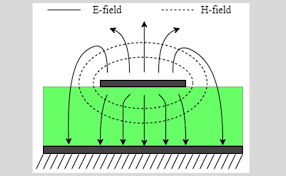
Signal loss in high-frequency circuits arises primarily from conductor and dielectric contributions, each dominating under specific conditions. Conductor losses occur due to the skin effect, where current flows near the trace surface at high frequencies, increasing effective resistance. Surface roughness on copper further exacerbates this by scattering the current path, leading to higher attenuation per unit length. As frequency rises, these effects compound, directly contributing to high-frequency signal loss.
Dielectric losses represent another major factor, driven by the material's dissipation factor (Df) and dielectric constant (Dk). The dielectric absorbs signal energy, converting it to heat, with loss proportional to frequency, Dk, and Df. In standard laminates, rising Df at gigahertz ranges amplifies this, causing signal attenuation PCB degradation over longer traces. Radiation losses also play a role in poorly controlled layouts, where signals couple to free space, but these are secondary to material effects.
Additional contributors include impedance mismatches and via transitions, which introduce reflections adding to overall loss. Temperature variations alter Dk and Df, worsening performance in operational environments. Engineers must quantify these through measurements to pinpoint dominant mechanisms during PCB design troubleshooting.
The Fundamentals of Low Dk PCBs and Their Benefits
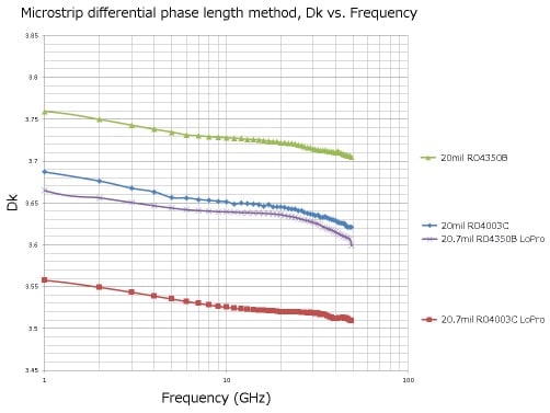
Low Dk PCB refers to printed circuit boards using laminates with a dielectric constant below typical values, often around 3.0 or less compared to 4.5 for standard epoxy glass. The Dk measures the material's ability to store electrical energy relative to air, influencing signal velocity and coupling. Lower Dk accelerates signal propagation, as velocity equals the speed of light divided by the square root of Dk, enabling tighter timing margins in high-speed designs.
Beyond speed, low Dk PCB benefits include minimized capacitive coupling between traces, reducing crosstalk in dense layouts. This proves vital for maintaining signal integrity in multilayer stacks where proximity heightens interference risks. In high-frequency applications, low Dk materials exhibit more stable properties across frequencies, preventing unexpected shifts that degrade performance.
Dielectric loss ties closely to Dk, as attenuation formulas incorporate both Dk and Df. Selecting low Dk/Df combinations curbs energy dissipation, directly addressing signal attenuation PCB concerns. Compliance with IPC-4101 standards ensures these materials meet specifications for base laminates, including controlled Dk values suitable for high-frequency use. Overall, low Dk PCBs support longer trace lengths before significant degradation occurs.
Related Reading: Prepreg Thickness & Dielectric Constant: Optimizing PCB Performance
Mechanisms of Signal Attenuation in Detail
To troubleshoot effectively, engineers dissect attenuation into quantifiable components using transmission line theory. For microstrip or stripline geometries, total loss α totals conductor loss αc, dielectric loss αd, and leakage. Conductor loss follows αc ≈ (Rs / Z0 * w), where Rs is surface resistance rising with square root of frequency due to skin depth δ = sqrt(2 / (ω μ σ)).
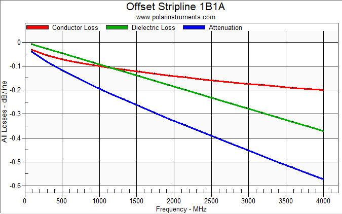
Dielectric loss computes as αd = (π f / c) * Df * sqrt(Dk), highlighting frequency's linear impact and Df's direct role. Low Dk reduces the sqrt(Dk) term modestly, but pairs best with low Df for optimal results. Surface roughness adds an extra factor, modeled via Huray model, amplifying losses by 20-50% in rough foils at 10 GHz.
Impedance control per IPC-2221 guidelines prevents reflections compounding attenuation. Variations from inconsistent Dk across the board cause standing waves, further eroding signal amplitude. Environmental factors like humidity swell dielectrics, elevating effective Dk and losses.
Practical Troubleshooting Steps for High-Frequency Signal Loss
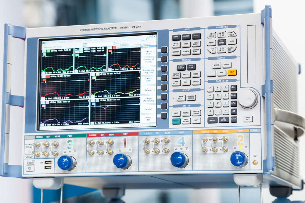
PCB design troubleshooting begins with vector network analyzer (VNA) measurements of S-parameters, focusing on S21 insertion loss. Compare measured curves against simulations to isolate material versus geometry issues. If dielectric loss dominates above 5 GHz, suspect high Df; steep slopes indicate conductor problems from roughness.
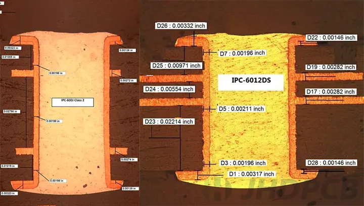
Time-domain reflectometry (TDR) reveals impedance discontinuities causing reflections. Correlate discontinuities with stackup or via locations for targeted fixes. Fabricate test coupons per IPC-4101 to characterize actual Dk/Df at operating frequencies, validating material specs.
For RF signal loss solutions, prototype iterations help: smooth copper, optimized stackups, and low Dk swaps. Thermal cycling tests uncover stability issues, as Dk drifts affect long-term performance. Document findings in design reviews to refine future layouts.
Best Practices for Low Dk PCB Implementation
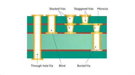
Adopt controlled impedance stackups with low Dk cores and prepregs, calculating widths via field solvers. Minimize vias using blind/buried types, and apply stitching for return paths. Route critical nets on inner layers shielded by ground planes to suppress radiation.
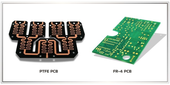
Select materials per IPC-4101 slash sheets specifying low Dk/Df grades for frequencies up to mmWave. Balance cost with performance, as low Dk often implies specialized resins. Fabricate with low-roughness copper foils reverse-treated for outer layers.
Validate designs through electromagnetic simulations incorporating measured material data. Enforce 3W spacing rules between traces to curb coupling. These RF signal loss solutions ensure robust high-frequency performance.
Related Reading: High Frequency PCB Design: How Core Thickness Affects Signal Loss and Performance
Case Study: Resolving Attenuation in a 10 GHz Design
Consider a radar module prototype exhibiting 3 dB excess loss at 10 GHz versus simulation. Initial VNA traces showed frequency-dependent roll-off pointing to dielectric issues. Stackup review revealed standard prepreg with Df > 0.01, replaced by low Dk/Df equivalent per IPC-4101 guidelines.
Post-change, loss dropped 1.5 dB, with TDR confirming uniform 50-ohm impedance. Conductor optimization via smoother foil added another 0.8 dB gain. Final validation met specs, highlighting low Dk PCB benefits in real troubleshooting.
This approach underscores systematic PCB design troubleshooting: measure, model, iterate.
Conclusion
High-frequency signal loss demands attention to both conductor and dielectric mechanisms for reliable circuits. Low Dk PCB benefits shine in reducing propagation delays, coupling, and attenuation, forming a cornerstone of RF signal loss solutions. By following structured PCB design troubleshooting—measurements, material swaps, and best practices—engineers achieve superior integrity.
Adhering to standards like IPC-2221 and IPC-4101 ensures designs meet industry benchmarks. Proactive material selection prevents common pitfalls, enabling innovation in demanding applications. Implement these strategies to elevate your high-frequency projects.
FAQs
Q1: What are the primary causes of high-frequency signal loss in PCBs?
A1: High-frequency signal loss stems from conductor losses via skin effect and roughness, dielectric losses from Dk and Df, and reflections from impedance mismatches. Frequency amplifies these, with dielectric dominating above 5 GHz. Troubleshooting involves S-parameter analysis to differentiate components. Low Dk materials mitigate dielectric contributions effectively.
Q2: How do low Dk PCB benefits improve signal attenuation PCB issues?
A2: Low Dk PCB benefits include faster signal velocity, reduced capacitive coupling, and lower dielectric loss when paired with low Df. This minimizes attenuation over long traces and stabilizes impedance. Engineers select per IPC-4101 for high-frequency suitability. Result: enhanced integrity without excessive cost.
Q3: What PCB design troubleshooting steps address RF signal loss solutions?
A3: Start with VNA for insertion loss and TDR for impedance. Test material Dk/Df via coupons. Iterate stackups with low Dk laminates and smooth copper. Simulate electromagnetic effects pre-fabrication. These steps per IPC-2221 yield reliable RF signal loss solutions.
Q4: When should engineers consider low Dk PCBs for high-frequency circuits?
A4: Opt for low Dk PCBs when operating above 1 GHz, facing >1 dB loss per inch, or needing precise timing. They excel in RF where standard materials falter. Verify via specs in IPC-4101. Balance with thermal and mechanical needs for optimal design.
References
IPC-4101 — Specification for Base Materials for Rigid and Multilayer Printed Boards. IPC, 2017
IPC-2221 — Generic Standard on Printed Board Design. IPC, 2012
IPC-4103 — Specification for High Frequency Base Materials. IPC