 ALLPCB


Introduction
High-frequency PCB design demands precise control over every aspect of the stackup to maintain signal integrity. As operating frequencies push beyond several gigahertz, even minor variations in materials and geometry can lead to unacceptable signal loss. Core thickness, a fundamental parameter in multilayer PCB construction, plays a pivotal role in determining overall performance. Engineers must understand how this dimension influences both conductor and dielectric losses to optimize high-speed PCB designs. This article explores the relationships between core thickness, signal attenuation, and key mechanisms like skin effect and dielectric loss. By examining PCB material properties and practical guidelines, designers can make informed choices for reliable high-frequency operation.
Understanding Core Thickness in Multilayer PCBs
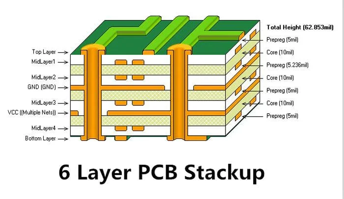
Core thickness refers to the dimension of the rigid dielectric laminate sandwiched between copper layers in a PCB stackup. These cores, typically fully cured resin systems, provide structural integrity and define the spacing between signal and reference planes. In high-frequency PCBs, the core separates conductive layers, directly affecting the characteristic impedance of transmission lines. Prepregs, which are semi-cured sheets, fill gaps between cores, but the core sets the primary dielectric height for stripline or embedded microstrip configurations. Variations in core thickness alter the electromagnetic field distribution around traces, influencing propagation characteristics. Proper selection ensures compliance with design rules outlined in standards like IPC-2221.
Thinner cores enable tighter coupling between planes, which supports higher layer densities in complex high-speed PCBs. However, mechanical constraints such as warpage and drilling tolerances must be considered during fabrication. Thicker cores offer greater rigidity but may introduce challenges in impedance control and thermal management. Engineers evaluate core thickness alongside overall board thickness to balance electrical and physical demands. This parameter becomes critical as frequencies increase, where signal wavelengths approach PCB dimensions.
Key Mechanisms of Signal Loss in High-Frequency PCBs
Signal loss in high-frequency PCBs arises primarily from two sources: conductor loss and dielectric loss. Conductor loss stems from the skin effect, where alternating current concentrates on the conductor surface at high frequencies, increasing effective resistance. This phenomenon scales with the square root of frequency, making it dominant above 1 GHz for typical copper traces. Dielectric loss occurs when the insulating material absorbs energy, quantified by the loss tangent or dissipation factor. PCB material properties like dielectric constant and loss tangent dictate the extent of this absorption. Together, these mechanisms contribute to insertion loss, degrading eye diagrams and bit error rates in high-speed signals.
The skin effect confines current flow to a depth δ = 1 / sqrt(π f μ σ), where f is frequency, μ permeability, and σ conductivity. For copper at 10 GHz, skin depth is roughly 0.66 μm, far less than standard foil thickness. Wider traces mitigate this by reducing resistance per unit length, but geometry constraints apply. Dielectric loss follows α_d ≈ (π f / c) * sqrt(ε_r) * tanδ * geometry factor, emphasizing low-loss materials. Signal attenuation compounds over trace length, demanding minimization from the outset. Understanding these principles guides stackup decisions in high-frequency PCB design.
How Core Thickness Influences Conductor Loss via Skin Effect
Core thickness indirectly governs conductor loss by dictating trace geometry for controlled impedance. Characteristic impedance Z0 ≈ (377 / sqrt(ε_eff)) * (w / h) for microstrip, where h is dielectric height related to core thickness. To maintain 50 Ω, thinner cores require wider traces, which lower series resistance and skin effect losses. Simulations show that halving h can reduce conductor attenuation by 20-30% through increased trace width, though exact values depend on frequency and materials. This trade-off favors thinner cores in high-speed PCBs for reduced signal loss.
However, excessively thin cores risk fabrication tolerances and crosstalk if planes are too close. Skin effect remains independent of dielectric but trace width optimization hinges on h. Engineers model these effects using field solvers to predict insertion loss curves. Thicker cores necessitate narrower traces for Z0, amplifying skin effect and elevating attenuation at high frequencies. Balancing core thickness optimizes conductor performance without compromising manufacturability.
Core Thickness and Dielectric Loss Considerations
Dielectric loss depends on the electric field penetration into the core material, modulated by its thickness. Thinner cores concentrate fields more uniformly, but the filling factor in striplines approaches unity regardless of h. Attenuation α_d shows weak dependence on thickness for uniform dielectrics, prioritizing low tanδ materials. Thicker cores extend field paths, potentially increasing total absorption over long traces, especially in broadband signals. PCB material properties like stable Dk across frequency minimize variations.
In practice, thicker overall stackups correlate with higher dielectric losses due to cumulative prepreg and core contributions. Standards such as IPC-6012 emphasize qualification for high-frequency performance, including dielectric integrity. Thinner cores pair best with ultra-low loss laminates to suppress tanδ effects. Engineers select cores where thickness aligns with frequency band, avoiding resonance issues. This approach sustains signal integrity in demanding applications.
Optimizing PCB Stackup: Core Thickness Best Practices
Effective high-frequency PCB stackup design starts with symmetric layering around the neutral axis to minimize warpage. Place signal layers adjacent to ground planes with thin cores for low inductance return paths, reducing radiation and crosstalk. Target dielectric heights of 3-5 mils for 50 Ω striplines at multi-GHz speeds, adjusting for material Dk. Use field solvers to iterate stackups, verifying insertion loss below -1 dB/inch at target frequencies. Incorporate hybrid cores with low-loss tops for RF sections and cost-effective bases elsewhere.
Fabrication guidelines limit minimum core thickness to ensure via reliability and plating uniformity. Pair thin cores with low-roughness copper to further tame skin effect. Validate designs through time-domain reflectometry for impedance and vector network analysis for S-parameters. Avoid abrupt thickness changes between layers to prevent mode conversion. These practices enhance high-speed PCB performance while adhering to industry norms.
Practical Insights: Troubleshooting Signal Attenuation
In real-world high-frequency PCB projects, unexpected attenuation often traces to suboptimal core selection. A common issue arises when standard cores introduce higher tanδ at elevated temperatures, exacerbating dielectric loss. Engineers troubleshoot by decomposing insertion loss into conductor and dielectric components via TDT/TDR measurements. Adjusting core thickness iteratively refines Z0 and reduces total loss without respinning layouts. Case examples show 15% attenuation improvement by thinning signal-ground cores from 8 to 4 mils.
Mechanical factors like CTE mismatch amplify issues in thin cores, leading to warpage per IPC-A-600 criteria. Mitigate with balanced prepreg schedules. For automotive radar at 77 GHz, ultra-thin cores with PTFE blends minimize signal loss. Always correlate simulations with prototypes, as surface roughness adds unmodeled conductor loss. These insights empower proactive design for robust high-speed PCBs.
Conclusion
Core thickness profoundly shapes signal loss profiles in high-frequency PCB design through its leverage on impedance, trace geometry, and loss mechanisms. Thinner cores generally reduce conductor losses via skin effect by enabling wider traces, while demanding low tanδ materials to control dielectric attenuation. PCB material properties must align with stackup choices for optimal performance. Adhering to structured best practices ensures minimal signal attenuation across frequencies. Engineers benefit from modeling, standards compliance, and validation to achieve reliable high-speed PCB outcomes. Mastering these elements elevates design quality in demanding applications.
FAQs
Q1: How does reducing core thickness impact skin effect in high-frequency PCBs?
A1: Reducing core thickness allows wider traces to maintain characteristic impedance, lowering effective resistance from skin effect. Current crowds to the conductor surface at high frequencies, but broader widths distribute it better, cutting conductor loss. This benefits signals above 5 GHz, though crosstalk risks increase. Pair with smooth copper foils for maximum gain in high-speed PCB designs.
Q2: What role do PCB material properties play with core thickness for signal attenuation?
A2: PCB material properties like dielectric constant and loss tangent interact with core thickness to determine dielectric loss. Thinner cores amplify the need for low tanδ to prevent energy absorption. Stable Dk ensures consistent propagation delay across the stackup. Optimizing both minimizes signal attenuation in high-frequency PCB applications.
Q3: Why choose thinner cores for high-speed PCB signal integrity?
A3: Thinner cores tighten plane coupling, supporting low-inductance returns and controlled impedance for high-speed PCBs. They enable trace geometries that combat skin effect losses effectively. However, balance with fabrication limits to avoid warpage. This choice reduces overall signal loss while enhancing density.
Q4: Can thicker cores ever benefit high-frequency PCB performance?
A4: Thicker cores provide mechanical stability in multilayer high-frequency PCBs, useful for high layer counts. They suit applications where rigidity trumps minimal loss, like power distribution. Yet, they often raise dielectric loss and require narrower traces, increasing skin effect. Evaluate per design frequency and constraints.


