ALLPCB


Introduction
High-power PCB design presents significant thermal challenges due to the heat generated by components such as power amplifiers, LEDs, and power converters. Excessive heat can lead to reduced reliability, performance degradation, and even failure through mechanisms like solder joint fatigue or laminate delamination. Effective thermal management relies on strategies that efficiently dissipate heat from hotspots to cooler regions, such as internal copper planes or external heatsinks. Among these, PCB thermal vias play a critical role by providing low-resistance paths for heat conduction. Blind and buried vias, in particular, offer advanced capabilities for targeted heat transfer in multilayer boards. This article explores their mechanisms, design considerations, and best practices to optimize blind via heat dissipation and buried via thermal conductivity in high-power PCB design.
Engineers designing for applications like electric vehicles or renewable energy systems must prioritize thermal pathways early in the layout process. Standard through-hole vias can sometimes introduce unwanted electrical parasitics or consume surface space unnecessarily. Blind vias connect surface pads to inner layers without penetrating the full board thickness, enabling precise blind via heat dissipation from components. Buried vias link internal layers exclusively, enhancing overall buried via thermal conductivity across the stackup. Together, these vias enable denser layouts while maintaining thermal integrity. Adhering to established guidelines ensures robust performance under demanding conditions.
Fundamentals of Vias in High-Power PCB Thermal Management
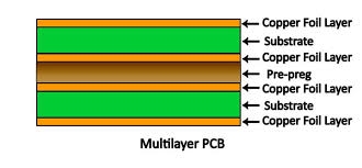
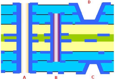
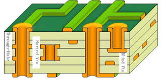
Vias in PCBs serve dual purposes: electrical interconnects and thermal conduits. In high-power applications, their thermal role becomes paramount as copper's high thermal conductivity, around 400 W/mK, far exceeds that of typical FR-4 substrates. Through-hole vias extend fully from one board surface to the other, providing straightforward heat paths but often requiring larger footprints. Blind vias terminate at an inner layer, ideal for surface-mount devices where heat needs to reach a specific plane without affecting the opposite side. Buried vias reside entirely within inner layers, invisible from the surfaces, and facilitate heat spreading between planes.
The choice between via types depends on board complexity and thermal requirements. In high-power PCB design, blind and buried vias support higher layer counts typical of HDI structures, freeing surface real estate for components. They minimize stub inductance, which benefits signal integrity alongside thermal benefits. However, their fabrication involves sequential lamination, increasing process steps compared to simple through vias. Understanding these differences guides engineers toward optimal configurations for PCB thermal vias. Proper implementation prevents thermal bottlenecks that could elevate junction temperatures beyond safe limits.
Thermal Mechanisms of Blind and Buried Vias
Heat dissipation in PCBs primarily occurs via conduction, convection, and radiation, with conduction dominating through solid materials like copper. PCB thermal vias leverage the copper barrel plating inside the drilled hole as the primary heat conductor, augmented by any fill material. For blind via heat dissipation, heat flows from a surface pad, through the via barrel, to an inner copper plane where it spreads laterally. This targeted path reduces thermal resistance compared to relying solely on in-plane conduction through thin dielectrics. The shorter aspect ratio of blind vias enhances plating uniformity, improving thermal performance.
Buried via thermal conductivity excels in multilayer boards by interconnecting power and ground planes directly. Heat enters the via from one inner layer, traverses the barrel, and exits to an adjacent plane, bypassing dielectric barriers. Arrays of such vias create effective vertical heat pipes, distributing load across multiple layers. In high-power PCB design, combining blind and buried vias forms a thermal network that equalizes temperatures. Factors like via diameter, plating thickness, and pitch influence overall efficacy, with denser arrays lowering effective thermal resistance. These mechanisms align with IPC-2221 guidelines for thermal relief in printed board design.
Related Reading: Thermal Management with Via in Pad: A Practical Approach
Design Best Practices for High-Power PCB Thermal Management
Effective high-power PCB design begins with strategic placement of PCB thermal vias near heat-generating components. Position blind vias directly under thermal pads of QFNs or BGAs to channel heat efficiently to inner planes. Use buried vias to link thick copper power planes, maximizing buried via thermal conductivity. Arrays of 4 to 16 vias, arranged in grids, provide redundancy and scale dissipation capacity without excessive density. Maintain consistent via sizes across the array to ensure uniform plating during fabrication.
Via filling enhances performance, especially for blind via heat dissipation. Conductive epoxy or copper fills increase cross-sectional area for heat flow while preventing solder wicking in assembly. For unfilled vias, tenting or plugging per IPC-4761 protects against contaminants and improves reliability. Consider stackup symmetry to avoid warpage from asymmetric thermal expansion. Simulate thermal profiles early to validate via configurations against expected power levels. These practices ensure compliance with thermal demands while supporting manufacturability.
Aspect ratios for blind and buried vias should stay below 1:1 to guarantee reliable plating, as steeper ratios risk voids. Staggered via patterns reduce stress concentrations during thermal cycling. Integrate vias with copper pours and embedded heat spreaders for hybrid solutions. Reference IPC-2152 for correlating current density with temperature rise in traces and vias. Iterative design refinement, informed by finite element analysis, optimizes blind via heat dissipation paths. Document all parameters in fabrication notes for consistent production.
Related Reading: The Benefits of Filling Blind Vias: Enhancing Reliability and Thermal Performance
Challenges and Troubleshooting in Via-Based Thermal Management
Implementing blind and buried vias introduces fabrication challenges like laser drilling precision and sequential build-up alignment. Misregistration can create open vias or plating defects, compromising buried via thermal conductivity. High-power operation exacerbates issues through electromigration in thin plating under sustained currents. Engineers must specify via protection types to mitigate solder entrapment or contamination risks.
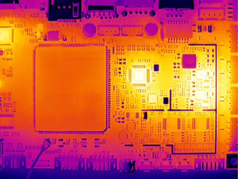
Troubleshooting starts with reviewing drill and fill charts against design rules. Thermal imaging post-assembly reveals hotspots indicating insufficient blind via heat dissipation. Adjust array density or add filled vias iteratively. Reliability testing simulates operating conditions to verify junction-to-ambient performance. Address warpage by balancing copper distribution across layers. These steps resolve common pitfalls in high-power PCB design.
Conclusion
Blind and buried vias are indispensable for thermal management in high-power PCBs, enabling efficient PCB thermal vias through targeted conduction paths. Blind vias excel in surface-to-inner heat transfer, while buried vias enhance interlayer spreading, collectively lowering thermal resistance. Adopting best practices like arrays, filling, and standards compliance ensures reliable performance. Engineers benefit from denser, cooler designs without sacrificing integrity. Prioritizing these elements from concept to production yields robust solutions for demanding applications.
FAQs
Q1: What are PCB thermal vias and their importance in high-power PCB design?
A1: PCB thermal vias are plated holes designed to conduct heat from components to other board layers or heatsinks, crucial for preventing hotspots in high-power applications. They leverage copper's superior conductivity to manage temperatures effectively. In multilayer boards, arrays of these vias distribute heat evenly, improving reliability and lifespan. Proper design per industry guidelines avoids common failures like delamination.
Q2: How do blind vias contribute to heat dissipation?
A2: Blind via heat dissipation occurs by connecting surface pads to inner planes without full board penetration, offering shorter, efficient paths. This targets heat from power devices precisely, reducing resistance compared to through vias. Filling enhances performance by increasing thermal mass. They support dense layouts in HDI PCBs while maintaining thermal integrity.
Q3: What role does buried via thermal conductivity play in multilayer boards?
A3: Buried via thermal conductivity links inner layers directly, bypassing dielectrics to spread heat across planes effectively. Ideal for high-power PCB design, they form vertical conduits in stackups. Arrays amplify capacity without surface impact. Protection methods ensure long-term reliability under cycling.
Q4: When should engineers use blind and buried vias over standard through vias?
A4: Opt for blind and buried vias in high-power PCB design needing density and targeted blind via heat dissipation. They minimize parasitics and free surface space. Through vias suit simpler boards, but advanced applications demand their precision. Evaluate via fabrication capabilities early.
References
IPC-2221C — Generic Standard on Printed Board Design. IPC, 2023
IPC-2152 — Standard for Determining Current Carrying Capacity in Printed Board Design. IPC, 2009
IPC-4761 — Design Guide for Protection of Printed Board Via Holes. IPC, 2021
IPC-6012E — Qualification and Performance Specification for Rigid Printed Boards. IPC, 2017