 ALLPCB


Introduction
In modern high-speed electronics, signal integrity challenges dominate PCB design considerations. Reference planes serve as foundational elements in impedance control PCBs, directly influencing the quality of signal return paths. Electric engineers must prioritize PCB reference plane impedance to prevent reflections, crosstalk, and attenuation that degrade performance. These planes, typically ground or power layers, form the low-inductance counterpart to signal traces, enabling controlled characteristic impedance. As data rates climb into gigabits per second, understanding signal return path PCB dynamics becomes essential for reliable operation. This article delves into the engineering principles, practical implementation, and optimization strategies for reference planes.
Defining Reference Planes and Their Core Functions
Reference planes in PCBs are dedicated conductive layers, usually copper, that act as voltage references for signal traces. They provide a stable, low-impedance path for return currents, completing the current loop essential for high-frequency signal propagation. In impedance control designs, these planes define the transmission line geometry alongside the trace and dielectric. Without a solid reference plane, signals experience increased loop inductance, leading to higher characteristic impedance variations. Engineers configure stackups to position signal layers adjacent to reference planes, forming microstrip or stripline structures. This setup ensures predictable electromagnetic fields confined between the trace and plane.
The distinction between ground and power reference planes arises from their roles in the circuit. Ground planes connect to the system's common reference, offering the lowest impedance path due to extensive via stitching and decoupling. Power planes distribute voltage but introduce higher effective impedance from current gradients and decoupling capacitors. Both contribute to signal return path PCB integrity, yet selection depends on layer adjacency and frequency content. IPC-2141A outlines guidelines for selecting reference planes in high-speed controlled impedance boards, emphasizing continuity and proximity.
Signal Return Paths: The Physics Behind Reliability
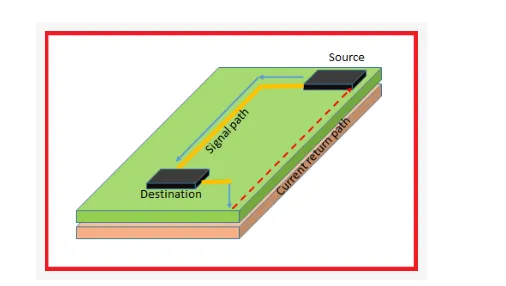
Every forward-propagating signal current generates an equal return current flowing in the opposite direction through the nearest low-impedance path. In PCBs, this return path follows the path of least inductance, typically the reference plane directly beneath the signal trace. Disruptions like plane splits force detours, increasing inductance and causing impedance discontinuities. This phenomenon manifests as ringing, overshoot, or eye diagram closure in time-domain reflectometry measurements. Maintaining continuous signal return path PCB structures minimizes these effects, preserving waveform fidelity across the board.
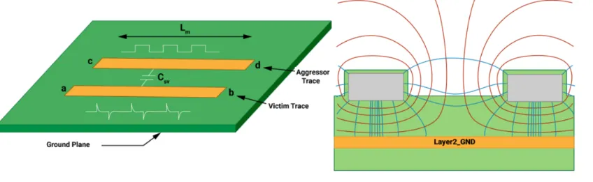
Electromagnetic field theory governs this behavior, where the return current spreads under the trace to minimize loop area. For differential signals, balanced return paths on adjacent planes enhance common-mode rejection. Variations in reference plane material or thickness alter field distribution, impacting capacitance and thus impedance. Engineers model these interactions using field solvers to predict Z0, the characteristic impedance. Solid planes outperform hatched or partial fills, as gaps elevate effective impedance by reducing capacitance.
PCB Reference Plane Impedance: Key Influencing Factors
PCB reference plane impedance refers to the effective impedance seen by return currents, influenced by plane thickness, surface roughness, and proximity to other layers. Thinner planes or those with anti-pad clearances around vias exhibit higher impedance due to restricted current flow. Dielectric height between signal and reference layers dominates impedance calculation, following Z0 = (87 / sqrt(εr + 1.41)) * ln(5.98h / (0.8w + t)) for microstrip approximations. Reference plane discontinuities, such as splits for routing power nets, create high-inductance barriers exceeding 1 nH per gap.
Power plane impedance often exceeds ground plane impedance because of non-uniform voltage drops from load currents. Decoupling capacitors bridge these planes, but their placement affects local impedance profiles up to hundreds of MHz. In multilayer boards, inter-plane capacitance further stabilizes return paths. Engineers verify compliance through time-domain reflectometry or vector network analysis during fabrication. Consistent plane design aligns with IPC-2221B requirements for generic printed board design, ensuring manufacturability.
Ground Plane Impedance vs. Power Plane Impedance
Ground planes excel as primary references due to their uniform potential and stitching vias that maintain low impedance across frequencies. They provide shielding against crosstalk by absorbing fringing fields from adjacent traces. Power planes, while viable references, suffer from dynamic impedance variations as current demands shift, potentially doubling effective Z compared to ground. Using a power plane as reference requires adjacent ground planes for bypass, forming a low-inductance pair.
In stripline configurations, signals between ground and power planes benefit from dual referencing, balancing capacitance. However, voltage differences across power planes induce noise coupling if not decoupled adequately. Ground plane impedance control prioritizes full pours with minimal cuts, while power planes tolerate islands for voltage domains. Simulations reveal that ground-referenced microstrips maintain tighter Z0 tolerances, often within 10% variation. Selection hinges on stackup symmetry and signal bandwidth.
Related Reading: Power Plane Impedance Control: Achieving Signal Integrity in High-Speed PCBs
Best Practices for Impedance Control PCB Grounding
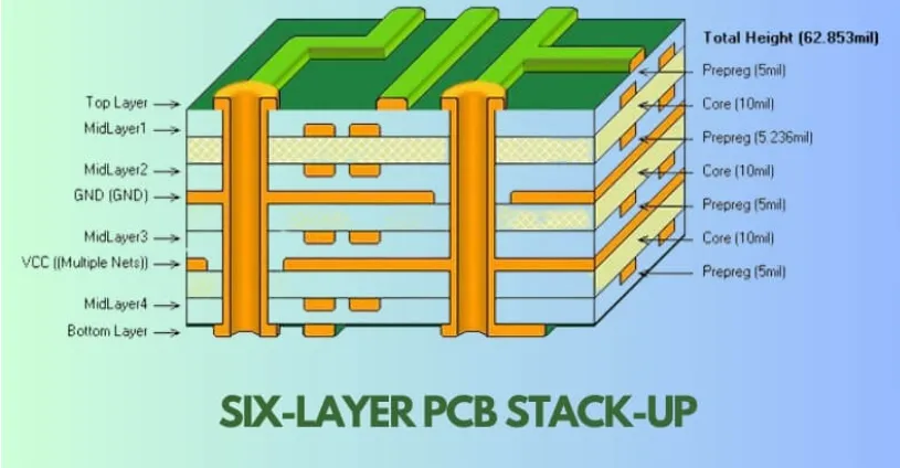
Position signal layers immediately adjacent to solid reference planes to minimize dielectric height and loop inductance. Avoid routing high-speed traces over plane splits; instead, use stitching vias every quarter wavelength to bridge gaps. For impedance control PCB grounding, prioritize dedicated ground planes on inner layers L2 and L5 in eight-layer stackups. Maintain plane continuity by routing splits parallel to traces or using moats with dense via fences.
Decouple power and ground planes with arrays of capacitors sized for target frequencies, placed under ICs. Verify stackup symmetry to prevent warpage impacting plane-to-trace spacing. Fabricate test coupons with daisy-chain traces for TDR validation post-lamination. Hatching planes only for flex regions, as it raises impedance by 5-15% versus solids. These practices ensure signal return path PCB robustness across thermal cycles.
In multi-voltage designs, segment power planes but flood unused areas to ground, enhancing overall shielding. Simulate via transitions with 3D solvers to quantify stub effects on return paths. Adhere to layer sequencing: signal-ground-signal-power for optimal impedance control.
Related Reading: PCB Grounding Techniques: A Guide to Minimizing Noise and Ensuring Reliable Connections
Troubleshooting Reference Plane Issues
Engineers encounter impedance mismatches when reference planes exhibit voids from plating defects, elevating return path inductance. Eye diagrams showing pre-shoot indicate split-plane routing; remedy by rerouting or adding vias. Excessive crosstalk arises from thin dielectrics without plane shielding, resolved by increasing separation or adding guard traces. Power plane resonance, evident as periodic noise, demands broader decoupling spectra.
Fabrication tolerances in plane etch uniformity cause Z0 drift; specify tighter controls per class 3 requirements. Thermal expansion mismatches warp boards, altering plane spacing; model CTE differences early. Field probing reveals return path deviations, guiding iterative fixes. Systematic stackup reviews prevent these pitfalls.
Conclusion
Reference planes underpin impedance control in PCBs by furnishing low-inductance signal return paths. Ground planes offer superior performance over power planes for most high-speed applications, demanding continuous pours and strategic via placement. Mastering PCB reference plane impedance, signal return path PCB design, ground plane impedance, power plane impedance, and impedance control PCB grounding elevates board reliability. Electric engineers applying these principles achieve robust signal integrity, aligning with industry benchmarks. Future designs will leverage tighter tolerances as frequencies rise, reinforcing the enduring role of reference planes.
FAQs
Q1: What is the primary role of a ground plane in signal return path PCB designs?
A1: The ground plane provides the lowest impedance return path for high-speed signals, minimizing loop inductance and reflections. It confines electromagnetic fields, ensuring controlled characteristic impedance in microstrip and stripline structures. Continuous ground planes under traces prevent detours that degrade signal integrity, and proper stitching maintains uniformity across the board.
Q2: How does PCB reference plane impedance affect overall performance?
A2: PCB reference plane impedance influences return current distribution, directly impacting trace Z0 stability. Discontinuities like splits increase effective inductance, causing overshoot and jitter. Solid planes lower this impedance compared to hatched fills. Engineers model and verify the stackup to hold impedance within specification.
Q3: Can power planes serve as effective references for impedance control?
A3: Power planes can reference signals but typically exhibit higher impedance than ground due to current gradients. Adjacent ground planes and proper decoupling mitigate this by forming low-inductance return paths. For gigahertz signals, ground planes are generally preferred as the primary reference, while stackup design balances both in multilayer boards.
Q4: What best practices ensure impedance control PCB grounding?
A4: Use adjacent solid reference planes, avoid splits under traces, and add stitching vias at transitions. Place dense decoupling between power and ground near loads, simulate the stackup for Z0 prediction, and fabricate test structures for TDR validation. These actions maintain return path continuity and suppress EMI.
References
IPC-2141A — Design Guide for High-Speed Controlled Impedance Circuit Boards. IPC, 2004
IPC-2221C — Generic Standard on Printed Board Design. IPC, 2023
IPC-6012E — Qualification and Performance Specification for Rigid Printed Boards. IPC, 2017


