 ALLPCB


Introduction
Stencil design plays a critical role in surface mount technology assembly when components feature irregular pad layouts. Engineers often encounter footprints that deviate from standard rectangular or circular shapes, such as L-shaped thermal pads or multi-segment contacts on connectors. These configurations demand precise control over solder paste deposition to maintain joint integrity and avoid defects. Effective stencil aperture design directly influences paste volume, release efficiency, and overall process yield. Addressing these requirements early in the design phase helps prevent costly rework during production.
What Is Stencil Design for Odd-Shaped Components and Why It Matters
Stencil design for odd shaped components involves creating custom apertures that match non-uniform pad geometries while respecting solder paste behavior. Irregular pads appear in applications like power modules, RF connectors, and specialized sensors where mechanical or thermal requirements dictate unique shapes. The process requires balancing paste release with sufficient volume to form reliable fillets without bridging or insufficient wetting. Industry professionals recognize that poor aperture design leads to inconsistent solder joints and reduced assembly reliability. Mastering these layouts supports higher first-pass yields and consistent performance across production batches.
Technical Principles
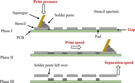
Solder paste transfer through a stencil follows fundamental fluid dynamics governed by aperture geometry and paste rheology. For irregular pads, engineers calculate the effective area ratio by dividing the aperture opening area by the wall surface area in contact with the paste. This ratio must remain above established thresholds to ensure clean release during separation. Aspect ratio considerations also apply, particularly when pad segments vary in width or include internal voids. Paste viscosity and particle size distribution further influence how the material flows into complex shapes. Structured evaluation of these parameters allows predictable deposition across diverse pad configurations.
Process variables such as squeegee pressure, speed, and angle interact with aperture design to determine final paste deposit quality. When pads feature angled or stepped profiles, localized pressure variations can cause uneven filling. Engineers therefore model paste behavior using computational tools to predict outcomes before physical stencils are produced. Consistent application of these principles reduces variability between boards and supports repeatable results in high-volume manufacturing.
Related Reading: Best Practices for Stencil Design in High-Volume SMT Assembly
Practical Solutions and Best Practices
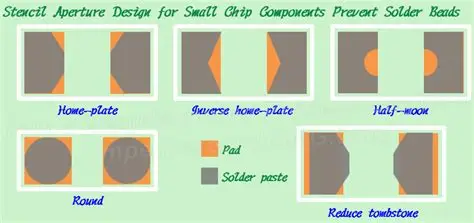
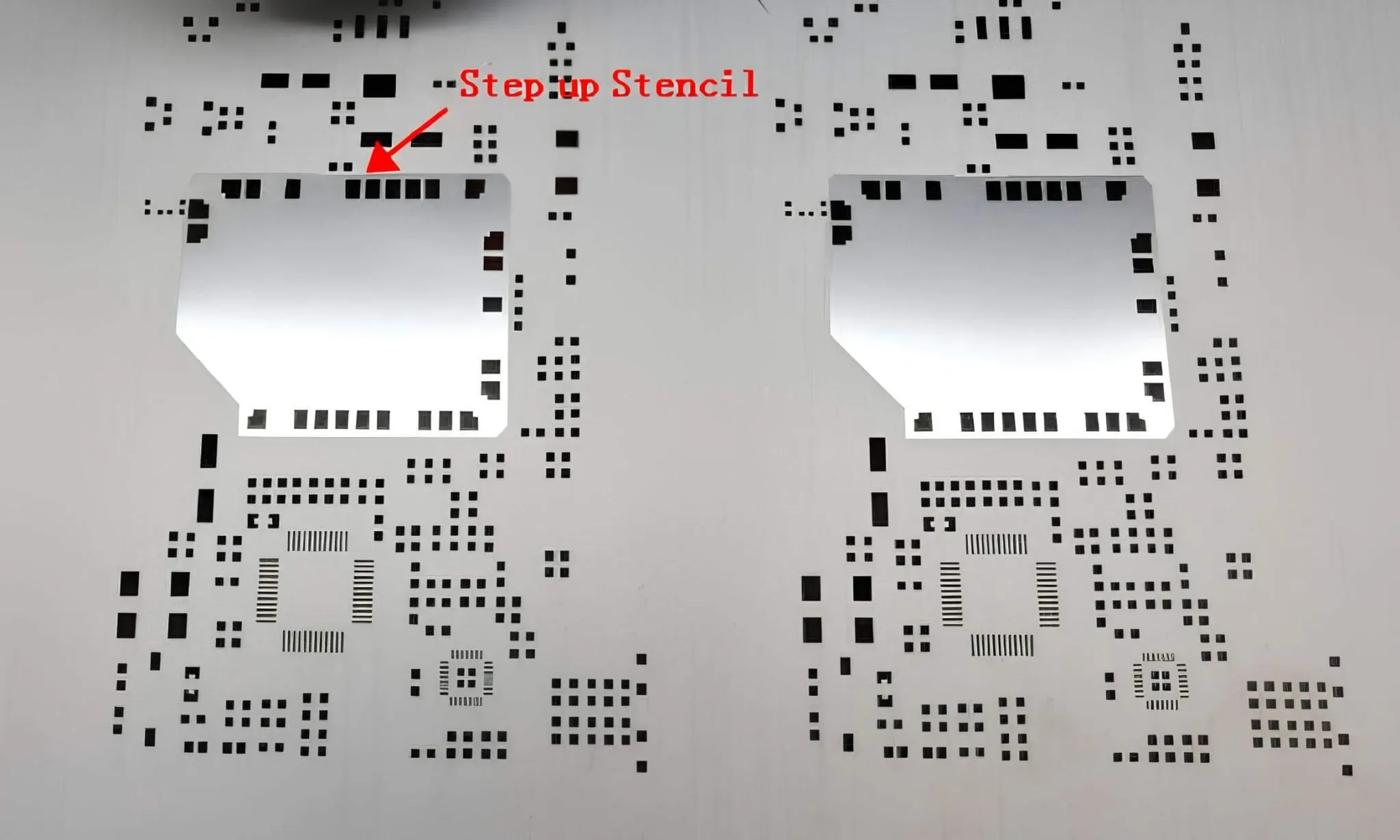
Custom stencil design begins with detailed footprint analysis to identify critical pad dimensions and required paste volumes. Aperture modifications, such as rounded corners or segmented openings, improve release while maintaining adequate solder for joint formation. Step-down or step-up stencil sections accommodate height differences between standard and irregular components on the same board. Engineers verify designs through area ratio calculations and adjust openings iteratively based on prototype results. These adjustments ensure compliance with assembly process windows without excessive trial runs.
Collaboration between design and process teams helps align stencil specifications with equipment capabilities and paste characteristics. Documentation of aperture dimensions, including any relief features or mesh patterns, supports traceability and future revisions. Regular review of deposition results against acceptance criteria allows fine-tuning that maintains quality across different production lots. Such disciplined approaches minimize defects associated with irregular pad layouts.
Related Reading: The Complete Guide to Stencil Design for PCB Assembly
Troubleshooting Insights
Common issues with stencil design for odd shaped components include paste bridging between closely spaced segments and insufficient volume on extended pad areas. Engineers diagnose these by examining deposit profiles after printing and correlating them with aperture geometry. Adjustments often involve increasing aperture size in narrow sections or adding relief cuts to reduce surface tension effects. Monitoring environmental factors such as temperature and humidity during printing further stabilizes outcomes. Systematic troubleshooting based on measured data leads to robust solutions that scale reliably.
Conclusion
Stencil aperture design for irregular pads requires careful application of engineering principles to achieve consistent solder paste deposition. By focusing on area ratio, aspect ratio, and custom modifications, engineers can address the unique challenges presented by odd-shaped components. Structured best practices and targeted troubleshooting support high-yield SMT assembly solutions. These methods ultimately contribute to reliable electronic products that meet performance expectations.
FAQs
Q1: What are the main stencil design challenges when working with odd shaped components?
A1: Stencil design challenges arise primarily from the need to balance paste volume and release efficiency on non-uniform pads. Engineers must account for varying geometries that affect how solder paste flows and separates from the stencil. Proper aperture sizing and shape adjustments help maintain joint quality while avoiding defects such as bridging or insufficient solder.
Q2: How does custom stencil design improve SMT assembly solutions for irregular pads?
A2: Custom stencil design allows precise matching of aperture openings to irregular pad layouts, resulting in more consistent paste deposits. This approach optimizes solder volume for each segment of the footprint and reduces variability during printing. The outcome is improved process control and higher assembly yields for components with complex pad shapes.
Q3: Why is area ratio important in stencil aperture design for irregular pads?
A3: Area ratio determines the ability of solder paste to release cleanly from the stencil aperture walls. For irregular pads, maintaining an adequate ratio ensures sufficient paste transfer without residue or incomplete filling. Engineers use this metric to guide aperture modifications that support reliable joint formation.
Q4: What role do industry standards play in stencil design for odd shaped components?
A4: Industry standards provide guidelines for acceptable paste deposition and joint quality that apply across various pad configurations. Following these references helps ensure designs meet established performance criteria for SMT processes. Consistent application supports traceability and repeatability in manufacturing environments.
References
IPC-7525B — Stencil Design Guidelines. IPC, 2018
J-STD-001H — Requirements for Soldered Electrical and Electronic Assemblies. IPC, 2020
IPC-A-610G — Acceptability of Electronic Assemblies. IPC, 2017


