 ALLPCB


In surface mount technology assembly, precise control over solder paste volume remains essential for achieving reliable joints across mixed component populations. Step-down stencils address this need by varying stencil thickness in targeted zones, allowing engineers to deposit the right amount of paste on fine-pitch pads while maintaining adequate volume on larger components. This approach directly supports SMT assembly efficiency and helps reduce common defects such as bridging or insufficient solder. Manufacturers who adopt step-down designs often observe measurable gains in first-pass yield without requiring additional equipment changes. The result is improved process stability that aligns with the demands of high-mix production environments.
What Step-Down Stencils Are and Why They Matter
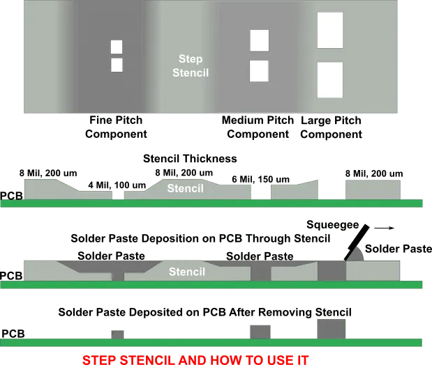
A step-down stencil consists of a single foil with locally reduced thickness in specific areas, typically created through chemical etching or laser machining. This construction enables selective control of solder paste release, particularly useful when boards combine ultra-fine-pitch devices with standard surface-mount parts. The technique improves solder paste control by limiting paste volume where excess material would cause shorts, while preserving full thickness elsewhere to ensure proper fillet formation. In practice, this flexibility supports reducing solder defects that otherwise require rework or scrap. Over time, the approach contributes to lower overall PCB manufacturing costs by minimizing material waste and inspection time.
Technical Principles Behind Step-Down Stencil Performance
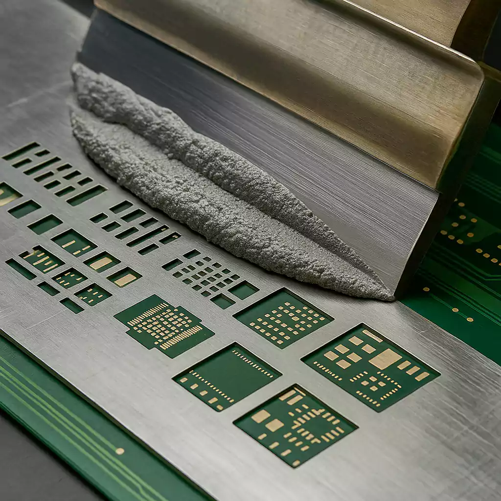
The core mechanism relies on the relationship between stencil aperture geometry and foil thickness. In full-thickness regions, paste fills the aperture completely and releases cleanly onto the pad. In stepped-down zones, the thinner foil reduces the volume transferred, which prevents excessive paste from accumulating on small pads. Engineers calculate the step location and depth based on component pitch and pad dimensions to maintain consistent print quality across the panel. Proper alignment between the step transition and the aperture edges is critical; misalignment can create paste scooping or incomplete release. When implemented correctly, the design maintains compatibility with standard squeegee angles and pressures used in most SMT lines.
Related Reading: Step Stencil vs. Standard Stencil: Which is Right for Your PCB?
Industry guidelines such as those from IPC emphasize the importance of matching stencil parameters to the specific solder paste and board finish. These recommendations help ensure repeatable deposition without introducing new variables into the printing process.
Practical Solutions and Best Practices for Implementation
Design teams begin by reviewing the bill of materials and identifying components that benefit from reduced paste volume. They then mark the corresponding regions on the stencil artwork and specify the step depth, commonly 0.05 mm to 0.10 mm less than the base foil thickness. During production, operators verify step registration using optical inspection before running the first boards. Regular cleaning of the stencil underside prevents paste buildup at the step edge, which could otherwise affect subsequent prints. When troubleshooting bridging on fine-pitch devices, engineers first confirm that the step-down area fully covers the affected apertures and that the squeegee pressure remains within the established window.
Process engineers also monitor paste height after printing to confirm that volume reduction in stepped areas stays within acceptable limits. Adjustments to print speed or snap-off distance can further optimize release in the thinner sections. These steps collectively enhance SMT assembly efficiency while supporting consistent quality across production runs.
Related Reading: Step Stencils: Optimizing Solder Paste Deposition for Mixed Component PCBs
Troubleshooting Common Issues with Step-Down Stencils
When insufficient solder appears on larger components, the first check is whether the step transition inadvertently overlaps those pads. Shifting the step boundary outward by a small margin often resolves the issue without redesigning the entire stencil. Conversely, if bridging persists on fine-pitch parts, increasing the step depth or adding a slight relief around the apertures can reduce paste volume further. Operators should also inspect for stencil warpage, as any distortion can alter the effective gap between foil and board. Maintaining proper storage and handling practices helps preserve the flatness required for accurate printing.
Documentation of each print run, including measured paste heights and defect counts, provides data for refining future designs. This iterative approach turns potential process problems into opportunities for improved control.
Conclusion
Step-down stencils deliver targeted solder paste control that enhances SMT assembly efficiency and supports reducing solder defects across diverse board layouts. By combining practical design rules with disciplined process monitoring, manufacturers achieve higher yields while managing PCB manufacturing costs more effectively. The technique integrates smoothly into existing lines and aligns with established industry practices for consistent results.
FAQs
Q1: How do step-down stencil benefits improve solder paste control in mixed-technology assemblies?
A1: Step-down stencils allow selective reduction of paste volume on fine-pitch pads while maintaining full volume on standard components. This targeted approach minimizes bridging and insufficient solder without changing the overall printing process. Engineers gain better process stability and fewer defects, which directly supports higher first-pass yields in SMT lines.
Q2: What role does a step-down stencil play in SMT assembly efficiency?
A2: By optimizing paste deposits for each component type on the same board, step-down stencils reduce the need for multiple print passes or secondary operations. Operators spend less time on rework and inspection, allowing lines to run at higher throughput. The design also helps maintain consistent quality across high-mix production schedules.
Q3: Can step-down stencils help with reducing solder defects on fine-pitch devices?
A3: Yes, the thinner sections of the stencil limit paste volume exactly where excess material would cause shorts or bridges. Proper step placement and depth ensure clean release while preserving adequate solder for reliable joints. This controlled deposition reduces common defects that otherwise require manual correction.
Q4: How do step-down stencils influence overall PCB manufacturing costs?
A4: Fewer defects mean less scrap and rework, which lowers direct material and labor expenses. Improved print consistency also reduces downtime for adjustments and inspection. Over multiple production runs, these savings accumulate without requiring investment in new equipment or processes.


