 ALLPCB


In-circuit testing plays a central role in modern PCB assembly lines, especially when manufacturers handle high-volume production runs. Engineers rely on this method to verify component placement and electrical connections right after the soldering stage. By catching defects early, teams avoid costly rework later in the process. Automated PCB testing systems integrate smoothly with existing assembly equipment, which helps maintain steady throughput without adding extra manual steps.
What Is In-Circuit Testing and Why It Matters
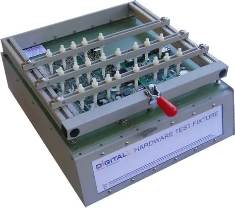
In-circuit testing, often called ICT, uses a bed-of-nails fixture or flying-probe system to check every node on a populated board. The test applies electrical signals to confirm that resistors, capacitors, and integrated circuits meet their specified values. This approach supports in-circuit testing process optimization because it runs in seconds per board, even on complex layouts. For ICT for high-volume PCB assembly, the speed and repeatability translate directly into fewer bottlenecks at the end of the line.
Industry standards such as IPC-A-610 guide the acceptance criteria that ICT systems use to flag defects. When production volumes increase, the ability to test boards quickly becomes essential for meeting delivery schedules. Teams that incorporate ICT early report measurable ICT efficiency gains through reduced scrap rates and shorter overall cycle times.
Technical Principles of In-Circuit Testing
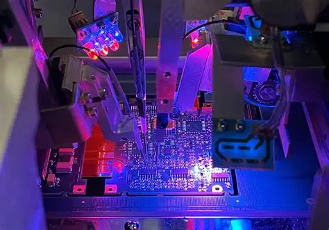
The core mechanism involves contacting specific test points on the board with spring-loaded probes. These probes measure resistance, capacitance, and continuity while the board remains powered down in most cases. Engineers design test points during the layout phase so that every critical node remains accessible. This structured access allows the tester to isolate faults such as open circuits, short circuits, or wrong-value components without powering up the entire assembly.
Troubleshooting becomes more straightforward because ICT pinpoints the exact location of a problem rather than requiring full functional testing. In high-volume environments, the system logs results automatically, which supports process monitoring and root-cause analysis. When combined with automated PCB testing software, operators can adjust parameters in real time to maintain consistent quality across batches.
Related Reading: The Role of In Circuit Testing in Ensuring PCB Reliability for Harsh Environments
Practical Solutions and Best Practices for Process Optimization
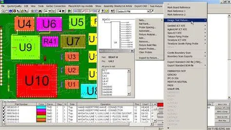
Successful integration starts with placing adequate test points during PCB design, typically at least one per net. Engineers review fixture drawings early to ensure probe access does not interfere with component placement or mechanical features. During production, regular calibration of the test system prevents drift that could lead to false failures. These steps contribute to reducing PCB assembly time with ICT by minimizing the need for repeated manual inspections.
Best practice also includes running boundary-scan tests alongside traditional ICT on boards that contain complex digital components. This hybrid method catches faults that simple continuity checks might miss. Teams schedule preventive maintenance on fixtures and probes to avoid unexpected downtime. When these practices are followed consistently, the overall assembly flow becomes more predictable and efficient.
Troubleshooting Insights in High-Volume Environments
Common issues arise when test points are too close to tall components or when solder mask covers access pads. Engineers address these by adjusting probe angles or adding dedicated test pads in the next revision. Another frequent challenge involves boards with dense layouts where probe interference occurs; in such cases, flying-probe systems often provide a flexible alternative to fixed fixtures. Monitoring first-pass yield data helps identify patterns that point to upstream process changes, such as stencil printing or reflow profiles.
Related Reading: Troubleshooting PCB In Circuit Testing: Common Problems and Solutions
Conclusion
In-circuit testing delivers clear efficiency gains when applied thoughtfully to PCB assembly. By verifying electrical integrity immediately after soldering, manufacturers reduce the volume of defective boards that reach later stages. Practical design choices and routine system maintenance keep the process reliable even as production volumes rise. The result is a more streamlined workflow that supports both quality and throughput goals.
FAQs
Q1: How does ICT support high-volume PCB assembly?
A1: In-circuit testing checks every node on each board in seconds, allowing continuous flow through the production line without manual intervention. This speed helps maintain output targets while catching component and connection faults early.
Q2: What steps improve in-circuit testing process optimization?
A2: Placing accessible test points during layout, calibrating fixtures regularly, and combining ICT with boundary-scan techniques reduce false calls and speed up fault isolation. These actions keep the overall assembly cycle time short.
Q3: Can automated PCB testing reduce PCB assembly time with ICT?
A3: Yes, automated systems log results instantly and flag defects for immediate rework, eliminating lengthy manual checks. The result is fewer delays between assembly stages and higher first-pass yields.
Q4: What ICT efficiency gains are typical in electronics manufacturing?
A4: Teams commonly see lower scrap rates and faster throughput because faults are isolated before boards move to functional or system-level testing. Consistent data collection also supports ongoing process improvements.
References
IPC-A-610G — Acceptability of Electronic Assemblies. IPC, 2017
J-STD-001G — Requirements for Soldered Electrical and Electronic Assemblies. IPC, 2017
ISO 9001:2015 — Quality Management Systems. ISO, 2015


