 ALLPCB


What Is Step Down Stencil Design and Why It Matters
Mixed technology PCBs combine surface mount devices with through hole components on the same board. This combination creates unique challenges during solder paste application because component leads and packages sit at different heights above the board surface. Engineers must control paste volume precisely to achieve reliable joints without defects such as insufficient solder or bridging. Step down stencil design addresses these height differences by varying the stencil thickness in specific zones. The approach improves solder paste deposition while maintaining coplanarity across the entire assembly.
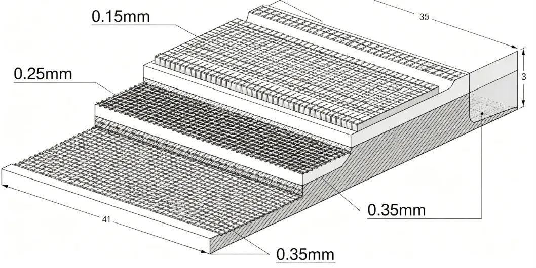
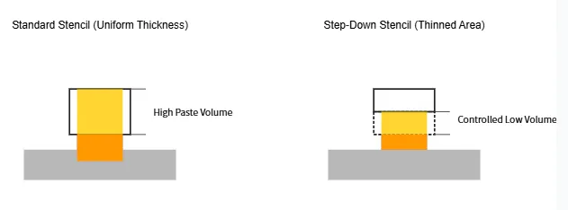
A step down stencil features localized reductions in foil thickness that align with taller components or leads. In mixed technology PCB layouts, these reductions prevent excess paste from being deposited on lower profile pads while still supplying adequate volume to higher features. Component height variation directly influences the required paste thickness, and uncontrolled variation leads to inconsistent solder joint formation. Solder paste deposition must therefore match the three dimensional profile of the board to avoid open joints or excess material that causes shorts. Coplanarity challenges arise when the stencil does not conform to these height differences, resulting in poor contact and uneven release.
Industry standards such as IPC A 610 emphasize the need for consistent solder volume to meet acceptance criteria for mixed assemblies. Proper step down design supports these criteria by tailoring paste amounts to each component type. Without this customization, manufacturers face higher rework rates and reduced first pass yields on boards that contain both fine pitch surface mount parts and robust through hole connectors.
Technical Principles and Mechanisms
Stencil printing relies on the relationship between aperture geometry, foil thickness, and squeegee pressure to control paste volume. In a step down region the thinner foil reduces the volume transferred to pads located beneath taller components. This volume reduction compensates for the additional space created by component leads or package bodies that sit above the nominal board plane. Engineers calculate the step depth based on the maximum component height difference and the desired paste aspect ratio.
Coplanarity challenges become pronounced when the board exhibits warpage or when components have varying lead coplanarity themselves. The stencil must maintain intimate contact with the pad surfaces across both thick and thin zones. Any gap allows paste to smear or prevents clean release, directly affecting deposition consistency. Mixed technology PCB designs therefore require careful mapping of all height critical features before stencil fabrication begins.
Solder paste rheology also interacts with step geometry. Higher viscosity pastes may not flow evenly into the transition areas between thick and thin sections, creating voids or inconsistent deposits. Designers address this by specifying gradual tapers or multiple discrete steps rather than abrupt thickness changes. These features promote uniform paste transfer while preserving the structural integrity of the stencil foil.
Related Reading: Designing Step Down Stencils for Fine Pitch QFNs: A Practical Guide
Practical Solutions and Best Practices
Designers begin by creating a detailed height map of all components on the mixed technology PCB. This map identifies zones requiring step down features and determines the exact depth needed to balance paste volume. Aperture sizes in the stepped regions are often enlarged slightly to maintain the target paste aspect ratio despite the reduced foil thickness.
During manufacturing, the stencil fabricator machines or etches the steps with tight tolerance on both depth and transition slope. Sharp transitions can trap paste or cause squeegee bounce, so smooth ramps are preferred. Engineers verify the finished stencil with optical or laser measurement tools to confirm that actual step depths match the design intent.
Process optimization includes adjusting squeegee pressure and speed when printing mixed height boards. Lower pressure in the thin zones prevents the foil from flexing excessively, while adequate pressure in the thick zones ensures complete aperture filling. Regular inspection of the first printed boards confirms that solder paste deposition meets volume targets across all component types.
Troubleshooting begins with paste volume measurements using automated inspection systems. Insufficient volume on lower pads points to excessive step depth, while bridging on taller features suggests insufficient step reduction. Iterative adjustments to step geometry, combined with aperture modifications, resolve most deposition issues without redesigning the entire stencil.
Related Reading: Step Down Stencils in SMT: Boost Performance and Cut Costs
Conclusion
Step down stencil design provides a reliable method for managing solder paste deposition on mixed technology PCBs that exhibit component height variation and coplanarity challenges. By tailoring foil thickness to the three dimensional profile of the assembly, engineers achieve consistent joint quality while reducing common defects. Careful height mapping, controlled step geometry, and process parameter optimization form the foundation of successful implementation. These practices align with established industry standards and support high yield production of complex boards.
FAQs
Q1: How does a step down stencil improve solder paste deposition on mixed technology PCBs?
A1: A step down stencil reduces foil thickness in zones above taller components, allowing precise control of paste volume. This adjustment compensates for component height variation and helps maintain uniform deposition across pads at different elevations. The result is improved joint formation and fewer defects related to excess or insufficient solder.
Q2: What role does coplanarity play in step down stencil performance?
A2: Coplanarity challenges arise when component leads or board surfaces sit at inconsistent heights. A properly designed step down stencil accommodates these variations by providing localized thickness changes that keep the stencil in contact with all pads. Without this accommodation, gaps form and paste release becomes inconsistent.
Q3: Why is component height variation a critical factor in mixed technology PCB assembly?
A3: Component height variation determines the amount of space available for solder paste between the stencil and each pad. Large differences require step down features to prevent over deposition on lower pads or under deposition on higher ones. Managing this variation ensures reliable electrical and mechanical connections.
Q4: What best practices help avoid common issues when using step down stencils?
A4: Engineers start with accurate height mapping and specify gradual step transitions. They verify stencil dimensions after fabrication and optimize printing parameters such as pressure and speed. Regular volume inspection on printed boards allows quick correction of any deposition inconsistencies.
References
IPC A 610H - Acceptability of Electronic Assemblies. IPC, 2020
J STD 001H - Requirements for Soldered Electrical and Electronic Assemblies. IPC, 2020
IPC 7525B - Stencil Design Guidelines. IPC, 2018


