 ALLPCB


Fine-pitch QFN components present unique challenges in surface-mount assembly because their small pad sizes and tight lead spacing demand precise control over solder paste deposition. Step-down stencil design addresses these challenges by selectively reducing stencil thickness in targeted areas, which directly influences the volume of solder paste transferred to each pad. Engineers rely on this approach to maintain consistent joint formation while minimizing defects such as bridging or insufficient solder. The technique integrates seamlessly into standard SMT processes when the stencil layout aligns with component footprint requirements and board layout constraints. Proper implementation supports higher yields and reliable electrical performance across production runs.
What Is Step-Down Stencil Design and Why It Matters
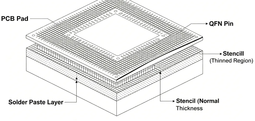
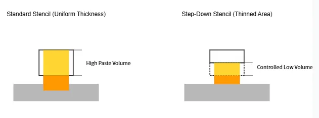
Step-down stencil design refers to a manufacturing method in which selected regions of the stencil foil are thinned to a lower thickness than the surrounding areas. This controlled reduction limits the amount of solder paste deposited on fine-pitch pads without altering the overall stencil thickness used for the rest of the board. For QFN components, where pad dimensions often fall below 0.5 mm pitch, the reduced paste volume helps prevent excess material from flowing between adjacent leads during reflow. Industry relevance stems from the increasing adoption of compact packages in consumer electronics, automotive modules, and industrial controls, where board real estate remains limited. Effective step-down designs therefore contribute to both assembly reliability and long-term product durability.
Technical Principles of Step-Down Stencil Design
The core mechanism involves calculating the required solder paste volume based on pad geometry and desired fillet height. Engineers determine the step-down thickness by comparing the calculated volume against the standard stencil thickness, then adjust aperture dimensions accordingly to maintain aspect ratios within acceptable limits. Solder paste rheology plays a central role because finer particles and specific flux formulations flow differently through reduced-thickness openings. When the stencil aperture area ratio drops below recommended thresholds, the step-down region compensates by lowering the height of the paste brick, which in turn reduces the risk of solder bridging between closely spaced QFN leads. Thermal expansion differences between the stencil foil and the PCB substrate must also be considered during design to ensure alignment remains accurate throughout the printing cycle. These principles derive from fundamental fluid dynamics and material science applied to stencil printing.
Related Reading: Step Stencil vs. Standard Stencil: Which is Right for Your PCB?
Best Practices for Implementing Step-Down Stencils with QFN Components
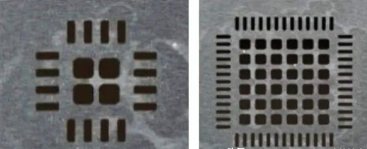
Designers begin by reviewing the QFN datasheet to identify exact pad dimensions and recommended land patterns before creating the stencil layout. Aperture openings in the step-down zone are typically kept at 80 to 90 percent of the pad width to balance paste release and volume control. The transition between full-thickness and step-down regions should follow a gradual taper rather than an abrupt edge to avoid stencil damage during repeated printing cycles. Engineers verify the final design through volume calculations that incorporate both the reduced thickness and the aperture geometry, confirming that the resulting paste deposit supports the target solder joint profile. Collaboration between the stencil fabricator and the assembly team ensures that foil material selection and etching tolerances align with the precision needed for fine-pitch applications. Regular inspection of printed boards after the first articles confirms that the step-down features perform as intended under production conditions.
Troubleshooting Common Issues in Fine-Pitch Stencil Applications
Insufficient solder volume often appears when the step-down thickness is reduced too aggressively relative to the aperture size. In such cases, increasing the aperture area slightly while maintaining the lower thickness restores adequate paste without introducing bridging. Conversely, excessive paste can occur if the step-down region does not cover the entire pad area, allowing full-thickness paste to remain on the outer edges. Engineers address this by extending the thinned zone to encompass the complete pad footprint and by confirming that the transition slopes do not trap paste. Misalignment between the stencil and the board can also amplify defects in fine-pitch QFN placements, so fiducial placement and stencil tensioning receive careful attention during setup. Systematic review of print quality after each adjustment helps isolate whether the root cause lies in stencil geometry, paste properties, or printer parameters.
Related Reading: Step Down Stencils in SMT: Boost Performance and Cut Costs
Conclusion
Step-down stencil design offers a reliable method for managing solder paste volume on fine-pitch QFN components when applied with careful calculation and adherence to established engineering practices. By integrating reduced-thickness zones with appropriately sized apertures, designers achieve consistent joint formation while reducing common assembly defects. The approach supports the broader goals of miniaturization and reliability that define modern electronics manufacturing. Continued attention to material properties, process parameters, and verification steps ensures that these designs deliver repeatable results across varying production volumes.
FAQs
Q1: How does step-down stencil design affect solder paste volume on QFN components?
A1: Step-down stencil design reduces the thickness of the foil in specific zones, which directly lowers the height of the deposited paste brick on fine-pitch pads. This controlled reduction helps achieve the target volume needed for reliable fillet formation without excess material that could cause bridging. Engineers calculate the exact thickness change based on pad size and desired joint profile to maintain process stability.
Q2: What aperture dimensions work best with fine-pitch stencil designs for QFNs?
A2: Aperture widths typically range from 80 to 90 percent of the pad width in the step-down region to optimize paste release while controlling volume. Length dimensions follow similar scaling to preserve aspect ratios that support clean separation from the stencil. These proportions are verified through volume modeling before the stencil is fabricated.
Q3: Why is stencil aperture ratio important when using step-down techniques?
A3: The aperture ratio determines how well paste releases from the stencil opening, and a low ratio can trap material even when thickness is reduced. Maintaining an appropriate ratio in the step-down zone ensures consistent deposition across all QFN pads. This balance prevents both insufficient and excessive paste that could compromise joint integrity.
Q4: How can engineers verify step-down stencil performance before full production?
A4: Verification begins with printed test boards that allow measurement of paste volume and deposit shape on representative QFN patterns. Visual inspection and automated paste inspection systems confirm that the reduced-thickness zones deliver the intended results. Adjustments to aperture size or step-down depth are made based on these measurements prior to committing to volume manufacturing.


