ALLPCB


SMT assembly processes rely on precise thermal management to achieve consistent solder joint formation across all components. Thermal relief features in pad design help control heat flow during reflow soldering, reducing the risk of defects that compromise board reliability. Engineers working on high-density layouts frequently encounter challenges related to uneven heating, and thermal relief provides a structured method to address these issues. Proper implementation supports both manufacturing yield and long-term product performance in demanding applications.
What Is SMT Pad Thermal Relief and Why It Matters
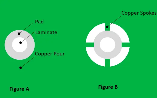
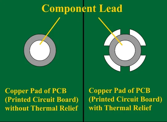
SMT pad thermal relief consists of narrow copper connections, often called spokes or bridges, that link the pad to the surrounding copper planes or traces. These connections limit the rate of heat dissipation into large copper areas during the soldering process. The approach maintains sufficient electrical and mechanical connectivity while allowing the pad to reach soldering temperature more uniformly. In high-volume production, this design choice directly influences defect rates and overall assembly quality.
Thermal relief becomes particularly relevant when components with small footprints, such as chip resistors or capacitors, are placed on boards with extensive ground or power planes. Without adequate thermal balancing, one side of a component may reflow before the other, leading to positional shifts or open joints. Industry standards such as IPC-2221 provide guidance on general printed board design practices that support these considerations. Engineers evaluate thermal relief early in the layout phase to align with overall board thermal profiles and reflow parameters.
Technical Principles and Mechanisms Behind Tombstoning
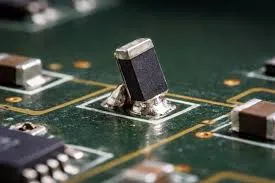
Tombstoning occurs when surface tension forces from molten solder lift one end of a passive component while the opposite end remains attached. The root cause often traces to differences in thermal mass between adjacent pads. A pad connected directly to a large copper plane absorbs heat more rapidly, delaying solder melt on that side relative to an isolated pad. This imbalance creates a torque that rotates the component into a vertical position.
Thermal relief mitigates the effect by reducing the cross-sectional area of copper between the pad and the plane. The narrower paths slow heat transfer without eliminating the electrical path required for signal integrity or power distribution. During reflow, both pads therefore reach the liquidus temperature of the solder alloy within a narrower time window. Controlled thermal gradients also help maintain consistent wetting angles and fillet formation across the joint.
Additional factors such as pad geometry, solder paste volume, and reflow oven profile interact with the relief design. Boards with mixed component sizes or varying copper densities require careful analysis of local thermal behavior. Simulation tools and thermal imaging during process qualification help validate that relief patterns achieve the intended balance.
Practical Solutions and Best Practices for Thermal Balance
Designers begin by identifying pads that connect to large copper areas and applying relief patterns only where thermal imbalance is expected. Common configurations use two or four radial spokes, each sized to carry the required current while providing thermal isolation. The relief pattern must still satisfy minimum conductor width rules to avoid electromigration or excessive voltage drop under operating conditions.
Process engineers coordinate with layout teams to ensure that stencil aperture design complements the relief geometry. Adequate paste deposition on both pads supports simultaneous reflow initiation. Reflow profiles are optimized with appropriate soak zones that allow heat equalization before the peak temperature stage. Regular review of first-article inspection data reveals whether adjustments to relief dimensions or spoke count improve outcomes.
When boards incorporate multiple plane layers, thermal relief should be applied consistently on inner layers as well as the outer surface. This prevents hidden heat sinking that could affect component behavior during double-sided assembly. Documentation of relief parameters in the fabrication notes helps maintain consistency across revisions and multiple production runs.
Related Reading: Copper Pour and Thermal Relief: A Guide to Preventing Soldering Issues
Troubleshooting Insights for Assembly Engineers
When tombstoning appears during production, the first diagnostic step involves reviewing the pad-to-plane connections on affected components. Engineers compare the copper distribution on each side of the component and note any asymmetry introduced by routing or plane fills. Increasing the number of spokes or slightly narrowing existing ones often restores thermal balance without redesigning the entire footprint.
Inspection under magnification after reflow can confirm whether solder has wetted both pads evenly. If one joint shows insufficient fillet height while the other appears normal, thermal relief adjustments combined with minor stencil modifications frequently resolve the issue. Process audits also check oven belt speed and zone temperatures to ensure the profile remains within the recommended window for the solder paste alloy in use.
Related Reading: How to Prevent Tombstoning in Components: Tips for Flawless Assembly
Conclusion
Effective SMT pad thermal relief design integrates electrical requirements with thermal management principles to minimize tombstoning and support reliable solder joints. By applying relief patterns selectively and validating them through process monitoring, engineering teams achieve higher first-pass yields and more robust assemblies. Consistent application of these techniques across product lines contributes to overall manufacturing efficiency and product longevity.
FAQs
Q1: How does SMT pad thermal relief design reduce the risk of tombstoning during reflow?
A1: Thermal relief limits heat flow from the pad into adjacent copper planes, allowing both ends of a component to reach soldering temperature at similar times. This reduces the surface tension imbalance that lifts one side of the part. Proper spoke sizing maintains current-carrying capacity while delivering the required thermal isolation.
Q2: What considerations guide the selection of thermal relief for tombstoning prevention in dense layouts?
A2: Engineers evaluate local copper density, component size, and expected reflow profile when deciding on spoke count and width. Relief patterns are applied primarily to pads connected to large planes. Coordination with stencil design ensures adequate solder paste volume on each pad.
Q3: Can soldering SMT pads with thermal relief affect signal integrity or power delivery?
A3: When designed correctly, thermal relief preserves the necessary electrical cross-section for the intended current and frequency range. Narrow spokes add minimal inductance or resistance compared with full plane connections. Verification through simulation or prototype testing confirms performance remains within specifications.
Q4: How does thermal balance SMT pads contribute to overall assembly quality?
A4: Balanced thermal behavior promotes uniform wetting and fillet formation on every joint. This consistency lowers defect rates and simplifies inspection criteria. Boards processed with attention to thermal relief exhibit improved reliability under thermal cycling and mechanical stress.
References
IPC-2221 — Generic Standard on Printed Board Design. IPC, 2003
J-STD-001 — Requirements for Soldered Electrical and Electronic Assemblies. IPC, 2020
IPC-A-610 — Acceptability of Electronic Assemblies. IPC, 2017