 ALLPCB


Tombstoning is a frustrating defect that can disrupt even the most carefully planned PCB assembly process. Picture this: a tiny surface-mount device (SMD), like a resistor or capacitor, standing upright on one end like a tombstone, disconnected from one pad and breaking the circuit. It's a common issue that engineers and manufacturers face, leading to unreliable solder joints, costly rework, and delays in production. The good news? With the right knowledge and techniques, tombstoning is entirely preventable. In this blog, we'll dive into what causes tombstoning, its impact on PCB assembly, and practical, actionable tips to ensure your SMD components stay perfectly in place. Whether you're designing a board or overseeing its assembly, these strategies will help you achieve flawless results.
Our goal is to equip you with insights that save time, reduce costs, and boost the reliability of your electronics. Let's explore the science behind tombstoning and uncover proven solutions to keep your PCBs performing at their best.
What Is Tombstoning and Why Does It Happen?
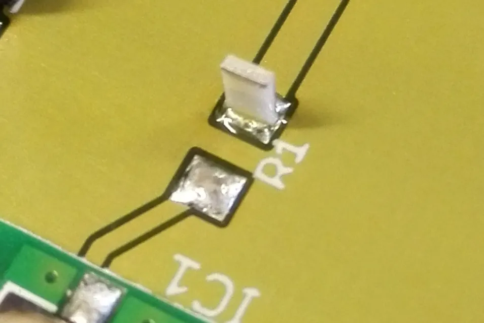
Tombstoning occurs when an SMD component lifts off one pad during soldering, leaving it attached only on the opposite end. Known as the 'Manhattan effect' or 'drawbridge effect,' this defect resembles a tombstone standing upright—hence the name. It's most common in small passive components, such as 0402 or 0201 resistors and capacitors, where even a slight imbalance can cause a big problem. The result? An open circuit that can render the component—and potentially the entire board—useless.
At its core, tombstoning is caused by uneven wetting forces during the reflow soldering process. Wetting happens when solder paste melts into a fluid state and bonds with the component's lead and the PCB pad. Ideally, the solder on both pads melts and solidifies simultaneously, securing the component evenly. But if one pad wets before the other, the surface tension pulls the component toward the wetter side, tilting it upward. Several factors can trigger this imbalance:
- Temperature differences: If one pad heats up faster—due to oven variations or thermal mass—it melts the solder first, creating uneven forces.
- Component size: Smaller components have less mass and surface area, making them more prone to lifting. For example, an 0201 package (0.6 mm x 0.3 mm) is far more susceptible than a larger 0805 package (2.0 mm x 1.25 mm).
- Pad design flaws: Unequal pad sizes or poor spacing disrupt uniform heating and wetting. A larger pad, for instance, may take longer to reach soldering temperature.
- Solder paste issues: Excess paste on one pad or uneven stencil application can accelerate wetting on one side.
- Surface finish variations: Finishes like Hot Air Solder Leveling (HASL) can leave uneven surfaces, affecting solder flow and increasing tombstoning risk.
Understanding these root causes is critical to preventing tombstoning. By tackling them head-on, you can ensure your components stay flat and functional.
The Impact of Tombstoning on PCB Assembly
Tombstoning isn't just a cosmetic flaw—it's a defect that can derail your entire project. Here's why it's a big deal for engineers and manufacturers:
- Open circuits: A lifted component breaks the electrical connection, causing immediate failure. In a complex circuit, this can halt functionality entirely.
- Higher costs: Reworking tombstoned boards adds labor and material expenses. In high-volume production, even a 1% defect rate can translate to thousands of dollars in losses.
- Reliability risks: Reworked joints may not be as strong, leading to failures down the line. For critical applications—like medical devices or automotive electronics—this is unacceptable.
- Lower yields: Tombstoning reduces the number of usable boards coming off the assembly line, forcing extra inspections or slower production to catch defects.
The stakes are high, especially when precision and uptime matter. Preventing tombstoning isn't just about avoiding headaches—it's about ensuring quality, efficiency, and customer satisfaction.
How to Prevent Tombstoning: Actionable Tips for Engineers and Manufacturers
Preventing tombstoning requires a mix of smart design choices and precise assembly practices. Below, we've outlined seven detailed strategies to keep your SMD components grounded. Each tip is backed by practical steps you can implement today.
1. Optimize Pad Design
Pad design is your first line of defense against tombstoning. Symmetrical, well-sized pads promote even wetting and heating.
- Stick to IPC standards: The IPC-7351 guideline recommends pad dimensions for SMD components. For an 0402 resistor, pads might be 0.5 mm x 0.6 mm with a 0.4 mm gap—check the spec for your package.
- Match pad sizes: If one pad is 20% larger, it heats slower, delaying wetting. Keep both pads identical in size and shape.
- Verify spacing: Too little space (e.g., <0.2 mm for 0201 parts) risks solder bridges; too much throws off balance. Match the component's footprint exactly.
2. Choose the Right PCB Surface Finish
Your PCB's surface finish affects how solder flows and wets. Uneven finishes can tip the scales toward tombstoning.
- Upgrade from HASL: HASL's uneven thickness (up to 50 µm variation) can disrupt solder flow. Switch to Electroless Nickel Immersion Gold (ENIG) or immersion tin for a flatter surface (variation <5 µm).
- Weigh cost vs. quality: ENIG costs more but excels with tiny components. For budget projects, OSP offers a decent compromise.
- Test your finish: Run a small batch to see how your chosen finish behaves with 0201 or smaller parts.
Recommended Reading: Surface Finishes Compared: ENIG, HASL, and Immersion Silver for PCBs
3. Ensure Uniform Solder Paste Application
Solder paste inconsistency is a tombstoning culprit. Too much paste on one pad—or too little—creates uneven forces.
- Refine stencil design: For 0402 components, use a 4-mil (0.1 mm) thick stencil with apertures sized at 90% of pad area to control paste volume.
- Check paste height: Aim for a uniform 0.1–0.15 mm thickness. Excess paste (e.g., 0.2 mm) can lift components during reflow.
- Use AOI: Automated optical inspection catches misprints before reflow, saving you from downstream defects.
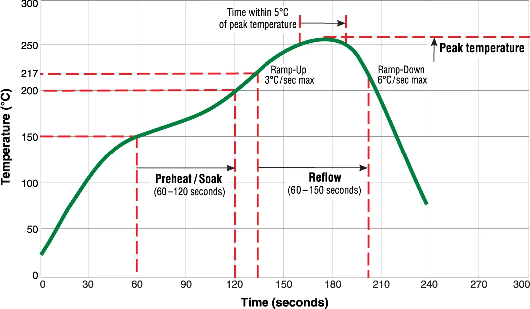
4. Control the Reflow Profile
A well-tuned reflow profile ensures both pads melt solder at the same time, avoiding imbalances.
- Slow the ramp-up: A rate of 1–2°C per second in the preheat zone (up to 150°C) prevents thermal shock. Rapid ramps (e.g., 4°C/s) risk uneven heating.
- Add a soak zone: Hold the board at 150–180°C for 60–90 seconds to equalize temperatures before hitting the reflow peak (e.g., 245°C for SAC305 solder).
- Calibrate your oven: A 5°C variation across zones can trigger tombstoning. Test with a thermal profiler regularly.
Recommended Reading: Reflow Soldering for Beginners: A Comprehensive Guide to SMT Assembly
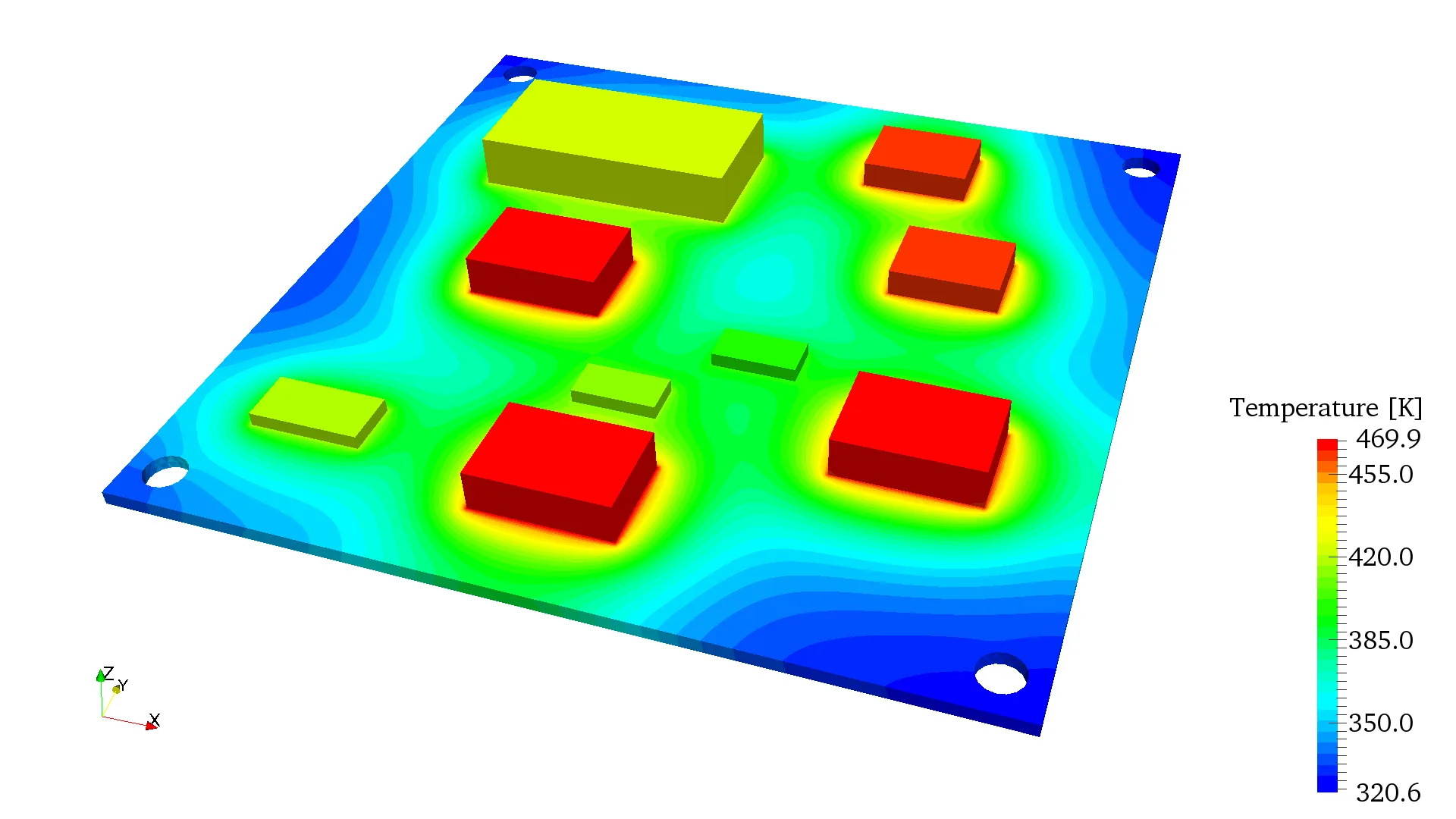
5. Balance Thermal Mass and Trace Design
Thermal mass differences—caused by traces or copper pours—can slow heating on one pad, inviting tombstoning.
- Symmetrize traces: If one pad connects to a 0.5 mm trace and the other to a 1 mm trace, the larger one acts as a heat sink. Match trace widths and orientations.
- Limit copper pours: A large copper area near one pad might drop its heating rate by 10–15%. Use thermal reliefs (e.g., 0.2 mm spokes) to isolate pads.
- Place vias wisely: A via 0.3 mm from a pad can sink heat. Keep vias >1 mm away or mirror them on both sides.
Recommended Reading: Thermal Management in PCB Design: Meeting Standards for Heat Dissipation
6. Select Components and Solder Wisely
Component size and solder type influence tombstoning risk. Make choices that favor stability.
- Favor larger packages: An 0603 part (1.6 mm x 0.8 mm) resists lifting better than an 0201 due to its mass (about 2 mg vs. 0.2 mg).
- Pick plastic-range alloys: SAC305 (melting range 217–220°C) transitions gradually, reducing wetting imbalance compared to Sn63/Pb37 (sharp 183°C melt).
- Test your combo: Reflow a sample board with your chosen components and solder to spot risks early.
7. Implement Design for Manufacturing (DFM) Checks
DFM catches tombstoning hazards before production starts, saving time and scrap.
- Simulate reflow: Tools like Altium or KiCad can model heat distribution, flagging pads with >10°C differences.
- Partner with assembly: Share your Gerber files with your manufacturer to review pad layouts and thermal balance.
- Iterate designs: A quick prototype run can reveal tombstoning trends—fix them before scaling up.
How ALLPCB Supports Flawless PCB Assembly
At ALLPCB, we're committed to helping you conquer challenges like tombstoning. Our advanced manufacturing capabilities deliver precision at every step, from pad fabrication to reflow soldering. With quick-turn prototyping, you can test your designs in days, tweaking pad layouts or thermal profiles to eliminate defects before full production. Our global logistics ensure your boards arrive fast, while our expertise in high-quality assembly—backed by ENIG finishes and optimized reflow processes—minimizes risks. Partnering with ALLPCB means you've got a team dedicated to turning your designs into reliable, high-performance PCBs.
Conclusion
Tombstoning doesn't have to haunt your PCB assembly process. By optimizing pad design, selecting the right surface finish, perfecting solder paste application, fine-tuning reflow profiles, balancing thermal mass, choosing stable components, and leveraging DFM checks, you can keep SMD components flat and functional. These steps not only cut defects but also boost yields, reduce costs, and ensure your electronics perform reliably—whether they're powering a gadget or a life-saving device. With these tips in hand, you're ready to build PCBs that stand the test of time, not stand up on their own.


