 ALLPCB


Sequential Lamination PCBs: Mastering Stack-Up Design for Signal Integrity
Sequential lamination enables the construction of complex multilayer printed circuit boards by bonding subsets of layers in multiple stages rather than a single operation. This approach supports the creation of high-density interconnect structures with blind and buried vias that would be difficult or impossible to achieve through conventional lamination. For electric engineers working on high-speed digital and RF designs, the technique directly influences the ability to maintain consistent electrical performance across the board. Proper implementation requires careful coordination between layer count, via placement, and material properties to meet both mechanical and electrical requirements.
What Is Sequential Lamination in PCBs and Why It Matters
Sequential lamination builds a PCB by laminating inner cores or subassemblies first, then adding outer layers in subsequent press cycles. Each cycle incorporates additional copper and dielectric materials while allowing the formation of vias that connect only specific layer groups. The process is particularly relevant for HDI constructions where fine-line features and dense via arrays are necessary. In applications involving high-frequency signals, this staged method provides greater flexibility in arranging signal layers relative to reference planes. Engineers select sequential lamination when conventional build-up methods cannot deliver the required via structures or impedance targets without excessive cost or reliability risks. The resulting stack-up directly affects transmission line behavior, return path integrity, and overall system noise margins.
Technical Principles of Stack-Up Design for Signal Integrity
Signal integrity in multilayer boards depends on maintaining controlled impedance, minimizing discontinuities, and ensuring low-loss return paths. Sequential lamination supports these goals by permitting asymmetric or hybrid via configurations that place critical signals adjacent to continuous ground or power planes. Dielectric constant and loss tangent of the prepreg and core materials determine propagation velocity and attenuation, while copper thickness and trace geometry set the characteristic impedance. Symmetry in the overall stack-up helps control warpage and stress during the multiple thermal cycles of lamination. Reference plane continuity must be preserved across lamination boundaries to avoid slots or gaps that increase inductance and crosstalk.
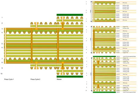
Impedance calculations for stripline or microstrip configurations incorporate the dielectric thickness between signal and reference layers as well as the trace width and spacing. Sequential lamination allows these thicknesses to be defined more precisely because inner layers are processed and inspected before outer layers are added. Any misalignment between lamination stages can shift via locations or alter dielectric spacing, which in turn affects impedance and timing skew. Engineers therefore specify tight registration tolerances and verify material properties before each press cycle. The choice of resin system and glass weave style further influences anisotropy and moisture absorption, both of which impact long-term electrical stability.
Related Reading: Unlocking HDI Potential: Mastering Sequential Lamination in PCB Design
Practical Solutions and Best Practices for Sequential Lamination Stack-Ups
Effective PCB stackup design sequential lamination begins with defining the minimum number of lamination cycles needed to achieve the required via structures. Limiting cycles to two or three reduces cumulative registration error and thermal stress while still enabling buried vias and fine-pitch routing. Signal layers are placed adjacent to solid reference planes whenever possible, with power planes positioned to provide low-impedance return paths for high-speed nets. Dielectric thicknesses are selected to achieve target impedances, typically 50 ohms single-ended or 100 ohms differential, using standard trace widths compatible with fabrication capabilities.
Symmetry about the board centerline remains a primary consideration to limit warpage after multiple lamination steps. Copper balance on opposite sides of the stack-up is maintained by mirroring signal and plane layers or by adjusting copper weights accordingly. Prepreg selection accounts for resin flow during each press cycle to ensure complete fill around vias and traces without excessive squeeze-out.
Related Reading: The Engineer's Guide to Sequential Lamination: Materials, Processes, and Best Practices
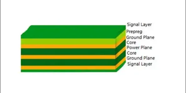
Impedance control sequential lamination requires collaboration between design and fabrication teams to confirm that the final pressed thicknesses match simulation models. Test coupons are often included on production panels to measure actual impedance after lamination. When HDI PCB stackup impedance control is critical, engineers specify low-loss materials and verify that the sequential process does not introduce additional roughness or resin-rich areas that alter effective dielectric properties. Thermal management considerations include ensuring that inner layers dissipate heat adequately during subsequent assembly reflow cycles.
Conclusion
Sequential lamination provides engineers with a powerful method for realizing complex stack-ups that support high signal integrity in dense, high-speed designs. By understanding the staged bonding process, material interactions, and the need for symmetry and reference plane continuity, designers can achieve consistent impedance and low crosstalk. Adherence to established industry practices ensures that the fabricated boards meet both electrical performance targets and mechanical reliability requirements. Careful planning of lamination cycles, dielectric selection, and via placement remains essential for successful outcomes.
FAQs
Q1: What role does sequential lamination play in PCB stackup design for signal integrity?
A1: Sequential lamination allows staged addition of layers and formation of blind or buried vias that support precise placement of signal traces next to reference planes. This arrangement helps maintain controlled impedance and reduces discontinuities that degrade high-speed signals. The process also enables use of optimized dielectric thicknesses between critical layers.
Q2: How does HDI PCB stackup impedance control benefit from sequential lamination?
A2: Sequential lamination permits inner layers to be processed and inspected before outer layers are bonded, improving accuracy of dielectric spacing that determines impedance. Engineers can achieve tighter tolerance on 50-ohm or differential pairs while incorporating complex via structures required in HDI designs. The staged approach also supports selection of low-loss materials suited to high-frequency performance.
Q3: Why is controlled impedance sequential lamination important for multilayer PCBs?
A3: Controlled impedance sequential lamination ensures that transmission line characteristics remain consistent across multiple press cycles. Proper planning of layer order, copper weights, and reference planes minimizes variations caused by registration shifts or resin flow. The result is predictable signal propagation and reduced risk of reflections or crosstalk in the final assembly.
Q4: What considerations apply to signal integrity PCB layers in sequential lamination builds?
A4: Signal integrity PCB layers in sequential lamination require continuous reference planes adjacent to high-speed traces and balanced copper distribution to limit warpage. Dielectric properties must be verified after each lamination stage because thermal history can affect final thickness and loss characteristics. Registration tolerances between stages directly influence via alignment and impedance repeatability.
References
IPC-2221B — Generic Standard on Printed Board Design. IPC, 2012
IPC-2226 — Sectional Design Standard for High Density Interconnect (HDI) Printed Boards. IPC, 2003
IPC-6012E — Qualification and Performance Specification for Rigid Printed Boards. IPC, 2020





