 ALLPCB


Introduction
Vias serve as essential vertical interconnects in printed circuit boards, enabling signals and power to travel between different layers. For electronic hobbyists starting with PCB design, mastering via placement ensures reliable connections without common pitfalls like signal loss or manufacturing defects. Proper via strategies simplify the routing process and improve overall board performance. This guide covers basic via placement guidelines, via types for beginners, via size selection, via spacing rules, and simple PCB via design techniques. By following structured approaches aligned with industry standards, hobbyists can create functional prototypes efficiently. Understanding these fundamentals builds confidence in multilayer board layouts.
What Are Vias and Why Do They Matter in PCB Design?
Vias are plated through-holes that provide electrical continuity across PCB layers, acting as bridges in multilayer constructions. In simple terms, they allow traces on one layer to connect to another without surface routing clutter. For beginners, vias matter because poor placement leads to fabrication issues, such as drill breakout or weak plating. They also influence signal integrity, thermal management, and board density. Hobbyists benefit from vias in projects like Arduino shields or sensor boards, where compact routing saves space. Adhering to basic via placement guidelines prevents costly respins during prototyping.
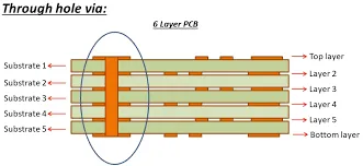
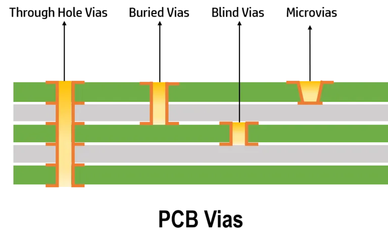
Via types for beginners primarily include through-hole vias, which span the entire board thickness, making them straightforward to implement. Blind vias connect an outer layer to an inner one, while buried vias link internal layers only, both saving space but requiring advanced fabrication. Through-hole vias suit most hobbyist designs due to their simplicity and compatibility with standard processes. Choosing the right type depends on layer count and routing needs. IPC-2221 outlines requirements for these interconnects to ensure reliability.
Understanding Via Types for Beginners
Through-hole vias represent the simplest option for beginners, drilled from top to bottom and plated to form a conductive barrel. They handle higher currents well and are easy to inspect visually. However, they consume more board real estate compared to advanced types. Blind and buried vias reduce via footprint but demand precise laser drilling or sequential lamination, which may exceed hobbyist budgets initially. Microvias, smaller than 0.15 mm, enable high-density designs but require specialized capabilities. Start with through-hole for simple PCB via design to build experience.
Each via type affects manufacturing yield and cost differently. Through-hole vias tolerate standard aspect ratios up to 10:1, where board thickness divided by hole diameter stays manageable. Blind and buried vias often limit to 1:1 or 0.8:1 for reliability. Hobbyists should consult fabricator capabilities before selecting types. Proper type selection aligns with project complexity, from single-layer power supplies to four-layer signal boards.
Basic Via Placement Guidelines
Strategic via placement minimizes routing congestion and enhances manufacturability. Position vias away from board edges by at least the minimum annular ring to prevent drill wander or breakout. Avoid clustering near high-heat components to reduce thermal stress on plating. In signal paths, place vias symmetrically for impedance control in hobbyist RF projects. Follow basic via placement guidelines by integrating vias into fanout patterns from components. This approach streamlines autorouting in design software.
Consider layer transitions carefully; unnecessary vias increase parasitic capacitance. Group vias for power and ground planes to form stitching, improving return paths. For multilayer boards, stagger via locations across layers to avoid alignment issues during lamination. These practices form the core of simple PCB via design. IPC standards like IPC-6012 provide qualification criteria for via integrity post-fabrication.
Related Reading: Via Placement for Beginners: Understanding Via Sizes, Types, and Spacing
Via Size Selection Principles
Via size selection balances current carrying capacity, aspect ratio, and density requirements. Larger drills accommodate more current but occupy space, while smaller ones suit fine-pitch routing. Factor in plating thickness, typically 25 microns, which reduces finished hole size. For hobbyists, select sizes compatible with standard drills to avoid premiums. Match via diameter to trace width for smooth transitions. Guidelines in IPC-2221 help determine appropriate dimensions based on external and internal layers.
Annular ring, the copper extension beyond the hole, ensures plating adhesion and breakout prevention. External layers need larger rings than internal for drill tolerance. Hobbyists often use 0.1 mm minimum rings initially for robustness. Test selections in simulations for high-speed signals. Consistent sizing across the board aids uniformity.
Via Spacing Rules and Considerations
Via spacing rules prevent electrical shorts, plating bleed, and mechanical weakness. Maintain center-to-center distances exceeding twice the drill diameter plus clearances. Edge-to-edge spacing avoids solder bridging in assembly. IPC-2221 addresses clearance for voltage levels, though hobbyist designs rarely exceed low voltages. In dense areas, use teardrops on via pads to reinforce connections. These rules integrate into design rule checks for error-free layouts.
Power and ground vias require wider spacing for heat dissipation. Stitching vias can be closer if non-functional overlaps are avoided. Fabricator DFM reports often specify minimums, typically aligning with Class 2 assembly. Hobbyists benefit from conservative spacing to maximize yield. Review spacing iteratively during routing.
Simple PCB Via Design Best Practices
Implement simple PCB via design by planning layer stackup first, assigning signals logically. Use through-vias for prototypes, transitioning to blind as skills grow. Tent unused vias on outer layers to protect from solder wicking. Back-drill if stubs affect high-speed signals, though unnecessary for most hobbyist work. Verify designs against IPC guidelines for compliance. These practices yield reliable boards with minimal iterations.
Incorporate thermal vias under power components, arrayed for even heat spread. Avoid via-in-pad for beginners unless filled and plugged. Document via counts per layer for quoting. Pair vias with decoupling caps near ICs for stability. Consistent application builds professional results.
Related Reading: Via Design in High Frequency PCBs: Minimizing Inductance and Signal Degradation
Common Mistakes and Troubleshooting for Hobbyists
Beginners often overcrowd vias, leading to spacing violations and yield drops. Oversized vias waste space; undersized ones risk open circuits from plating voids. Misaligned placements cause trace stubs, degrading signals. Troubleshoot by reviewing DRC violations and 3D renders. Adjust iteratively, consulting standards like J-STD-001 for soldering compatibility.
Another pitfall involves ignoring aspect ratios, causing plating inconsistencies in thick boards. Solution: limit to 8:1 for hobbyist fabs. Fabric defects like dog-boning show as tapered barrels; specify uniform plating. Learn from failed prototypes to refine future designs.
Conclusion
Mastering via placement transforms beginner PCB designs into robust, efficient boards. Key elements include via types for beginners, basic via placement guidelines, via size selection, via spacing rules, and simple PCB via design practices. Logical planning and standard adherence minimize errors. Hobbyists gain from starting simple, scaling complexity gradually. Apply these insights to elevate projects confidently.
FAQs
Q1: What are the basic via placement guidelines for hobbyist PCBs?
A1: Basic via placement guidelines recommend positioning vias away from edges, avoiding clusters near heat sources, and aligning with trace fanouts. This ensures manufacturability and signal integrity. Follow IPC-2221 for structured rules, integrating vias symmetrically in multilayer routing. Hobbyists achieve reliable prototypes by planning stackups first.
Q2: Which via types for beginners should I use in simple designs?
A2: Via types for beginners start with through-hole vias for their ease and current handling. Blind and buried suit denser boards later. Through-hole offers inspectability and standard compatibility. Select based on layer count, keeping aspect ratios low. This simplifies PCB via design effectively.
Q3: How do I approach via size selection for my PCB?
AX: Via size selection considers current needs, drill availability, and annular ring. Match to trace widths and plating reduction. Larger for power, smaller for signals. IPC guidelines provide class-based minima. Hobbyists test via arrays in prototypes for optimization.
Q4: What via spacing rules apply to beginner PCB layouts?
AX: Via spacing rules require center-to-center distances preventing shorts, typically per fabricator specs. Maintain clearances for voltage and plating. IPC-2221 covers electrical spacing. Stagger in planes for stitching. Conservative rules boost yields in simple PCB via design.
References
IPC-2221 — Generic Standard on Printed Board Design. IPC
IPC-6012E — Qualification and Performance Specification for Rigid Printed Boards. IPC, 2017
J-STD-001G — Requirements for Soldered Electrical and Electronic Assemblies. IPC, 2017


