ALLPCB


Introduction
Automotive electronics increasingly rely on printed circuit boards (PCBs) to control critical systems such as engine management, advanced driver-assistance features, and infotainment. The shift to lead-free manufacturing stems from global environmental regulations that restrict hazardous substances, pushing the industry toward fully lead-free processes. In automotive applications, this transition demands careful design to maintain reliability under harsh conditions like extreme temperatures, constant vibration, and thermal cycling. Automotive PCB lead-free designs must balance compliance with performance, as lead-free solders introduce unique challenges compared to traditional tin-lead alloys. Engineers face higher reflow temperatures and potential reliability risks, making proactive design essential. This article explores key considerations for achieving robust automotive PCB reliability in lead-free implementations.
Why Lead-Free PCBs Matter in Automotive Applications
Lead-free solders, typically tin-silver-copper alloys, replace tin-lead due to restrictions on lead use, aligning with broader sustainability goals in electronics. Automotive environments expose PCBs to severe stresses, including wide temperature swings, mechanical shocks from road vibrations, and humidity variations, where any failure can compromise vehicle safety. Automotive PCB lead-free adoption enhances environmental compliance while necessitating enhanced design strategies to match or exceed the ductility of leaded solders. Reliability becomes paramount, as solder joints must endure millions of cycles without cracking or fatigue. Industry standards guide this evolution, ensuring designs meet demanding qualification criteria. Ultimately, effective lead-free PCB design supports longer service life and reduces warranty claims in high-stakes automotive deployments.
The relevance intensifies with electrification trends, where power electronics generate additional heat, amplifying thermal demands on lead-free assemblies. Vibration from engines and drivetrains further tests mechanical integrity, highlighting the need for materials that resist deformation. Poorly designed lead-free boards risk warpage during assembly or premature failure in the field, underscoring the economic and safety imperatives. By prioritizing automotive PCB standards early, designers mitigate these risks and deliver systems that perform consistently.
Key Technical Challenges in Lead-Free Automotive PCB Design
Lead-free solders require higher melting points, around 217 degrees Celsius for common SAC305 alloys, compared to 183 degrees Celsius for eutectic tin-lead, leading to elevated reflow profiles that stress PCB materials. This increases the risk of warpage, particularly in multilayer boards, as base materials like standard FR-4 may soften near their glass transition temperature (Tg). Automotive PCB high temperature operation exacerbates this, with under-hood modules facing prolonged exposure to elevated ambient conditions. Coefficient of thermal expansion (CTE) mismatches between the PCB laminate, copper layers, and components generate shear stresses during thermal cycling, potentially cracking vias or delaminating layers. Engineers must model these interactions to predict long-term behavior.
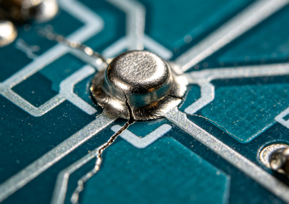
Vibration introduces dynamic loads that propagate through solder joints, where lead-free alloys exhibit brittleness due to their higher tin content. Random vibration profiles simulate real-world road conditions, causing fatigue in interconnects over time. Automotive PCB vibration resilience depends on joint geometry and pad design, as microcracks can initiate under repeated flexing. Combined with thermal stresses, this creates synergistic failure modes, demanding robust qualification testing. Material selection plays a pivotal role, as laminates with mismatched CTE values amplify strain at interfaces.
Solder joint reliability forms the core challenge, influenced by intermetallic compound formation during reflow. Lead-free processes promote thicker intermetallics, which are more prone to propagation under mechanical stress. In automotive contexts, where boards undergo shock and vibration, these compounds reduce compliance, accelerating crack growth. High-temperature excursions further degrade joint strength through creep mechanisms. Addressing these requires a holistic approach encompassing layout, materials, and process controls.
Related Reading: Lead Free PCB Design: Best Practices for High Frequency Applications
Material Selection for Enhanced Reliability
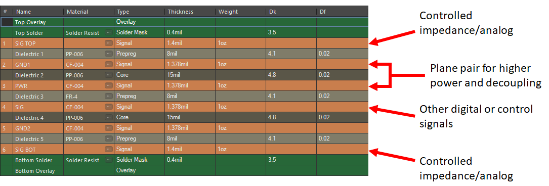
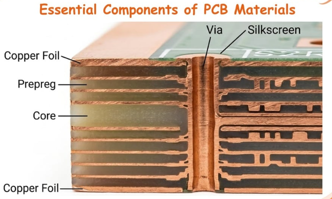
Selecting laminates with high Tg, typically above 170 degrees Celsius, prevents excessive board deformation during lead-free reflow and operational heat. These materials maintain dimensional stability, crucial for automotive PCB high temperature applications where junctions near engines reach demanding levels. Low-CTE cores minimize mismatch with silicon dies and ceramic components, reducing stress concentrations at solder interfaces. Hybrid stackups, combining high-Tg FR-4 with polyimide inner layers, offer balanced performance for mixed-signal boards. Copper foil type influences reliability, as reverse-treated foils adhere better under thermal stress.
Surface finishes must withstand lead-free assembly without compromising solderability. Immersion tin or organic solderability preservatives provide uniform wetting, essential for fine-pitch components common in automotive electronics. These finishes resist oxidation during multiple reflows, preserving joint integrity. Base material thickness impacts flex resistance, with thicker cores better suiting vibration-prone areas. Automotive PCB standards like IPC-6012DS specify qualification for such materials in high-reliability rigid boards.
Related Reading: PCB Material Selection: The Key to Effective Thermal Management
Layout and Stackup Strategies to Mitigate Stress
Symmetric stackups distribute thermal loads evenly, countering warpage tendencies in lead-free processes. Balanced copper distribution across layers prevents bowing, particularly in large panels used for automotive control units. Via placement requires annular rings sized to accommodate CTE-induced expansion, avoiding barrel cracks. Staggered vias in high-current paths enhance thermal dissipation while maintaining mechanical strength. Component orientation aligns sensitive parts away from board edges, minimizing vibration amplification.
Trace routing incorporates wider paths for power delivery, reducing resistive heating that compounds high-temperature risks. Controlled impedance lines for signal integrity account for material dielectric changes at elevated temperatures. Panelization strategies include fiducials for precise registration during assembly. These practices ensure automotive PCB reliability under combined thermal and mechanical loads.
Vibration and Thermal Management Best Practices
Effective thermal vias under hot components channel heat away from critical solder joints, vital for automotive PCB high temperature endurance. Copper planes act as heat spreaders, but their placement must avoid hotspots that induce localized CTE strain. Simulation tools model airflow and conduction, guiding pad array designs for optimal convection. Vibration countermeasures include anchoring points and conformal coatings to dampen resonances.
Solder paste volume control during stencil design ensures fillet formation that absorbs flex without fracturing. Mask-defined pads provide standoff, enhancing joint compliance. Post-assembly bake-out removes moisture, preventing popcorning in lead-free reflow. Qualification per IEC 60068-2 verifies performance under vibration and temperature extremes.
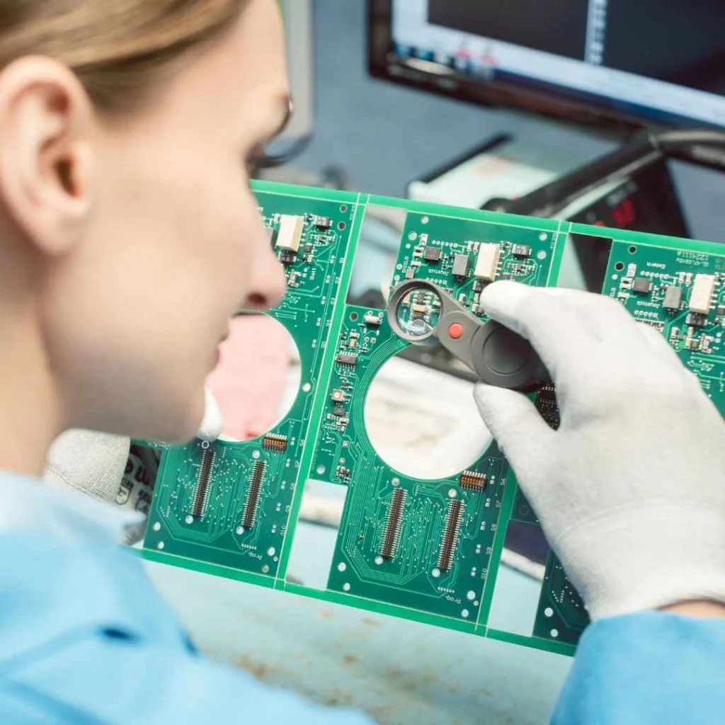
Practical Troubleshooting for Lead-Free Automotive PCBs
Warpage issues often trace to asymmetric copper or inadequate Tg, resolved by redesigning stackups and verifying flatness post-lamination. Solder joint cracks under vibration signal CTE mismatch, addressed by selecting compatible materials and reinforcing with underfill. High-temperature failures manifest as delamination, mitigated by high-Tg resins and controlled ramp rates in reflow. Reliability testing reveals early fatigue, prompting iterative layout tweaks. Field returns highlight process deviations, emphasizing adherence to automotive PCB standards like J-STD-001 for soldering.
Conclusion
Lead-free PCB design for automotive applications hinges on addressing thermal, mechanical, and material challenges through informed choices. High Tg laminates, CTE-matched stackups, and vibration-optimized layouts form the foundation of reliable assemblies. By integrating automotive PCB standards guidance, engineers ensure compliance and performance in demanding environments. Proactive strategies not only meet regulatory demands but elevate overall system robustness. Future advancements in alloys and materials will further refine these practices, sustaining innovation in vehicle electronics.
FAQs
Q1: What materials best support automotive PCB lead-free reliability?
A1: High Tg laminates exceeding 170 degrees Celsius prevent warpage during reflow and operation. Low-CTE cores match component expansion, minimizing solder stress. These selections align with IPC-6012DS for automotive rigid boards, ensuring endurance in thermal cycling and vibration. Practical testing validates joint integrity post-assembly.
Q2: How does vibration impact automotive PCB high temperature performance?
A2: Vibration fatigues brittle lead-free solder joints, accelerating cracks under thermal expansion mismatch. Robust pad designs and conformal coatings dampen effects. IEC 60068-2 testing simulates combined loads, guiding reinforcements. Proper layout reduces resonance, preserving automotive PCB reliability.
Q3: What role do automotive PCB standards play in lead-free design?
A3: Standards like J-STD-001 define soldering criteria for lead-free processes, specifying verification for high-reliability joints. They outline qualification for vibration and temperature, ensuring consistency. Compliance mitigates risks in automotive environments, supporting seamless integration.
Q4: Why prioritize CTE management in automotive PCB vibration designs?
A4: CTE mismatch induces shear at interfaces during flex and heat cycles, risking delamination. Matching laminate and component values distributes stress evenly. This enhances lead-free solder durability, critical for long-term vibration exposure in vehicles.
References
IPC-6012DS - Qualification and Performance Specification for Rigid Printed Boards as Addendum to IPC-6012D for Automotive Applications. IPC
J-STD-001 - Requirements for Soldered Electrical and Electronic Assemblies. IPC/JEDEC
IEC 60068-2 - Environmental Testing. IEC