ALLPCB


Introduction
High-frequency circuits open up exciting possibilities for electronic hobbyists, from building simple RF projects to experimenting with impedance matching for antennas. However, achieving reliable performance at home requires attention to impedance control, which prevents signal reflections and losses that can ruin your DIY high-frequency circuits. Many hobbyists overlook this when etching PCBs at home, leading to poor signal integrity in projects operating above 100 MHz. This guide focuses on impedance control for hobbyists, providing practical steps to design and build impedance controlled PCBs at home using basic materials and tools. By understanding the basics, you can create functional simple RF projects without professional equipment. Let’s explore how to make impedance matching straightforward and effective.
What Is Impedance Control and Why It Matters for Hobbyists
Impedance control refers to designing PCB traces to maintain a consistent characteristic impedance, typically 50 ohms or 75 ohms for RF applications. In high-frequency signals, mismatches cause reflections that distort waveforms, reduce power transfer, and increase electromagnetic interference. For DIY high-frequency circuits, this is crucial because hobbyist projects like antenna feeds or basic transmitters rely on clean signal paths. Without proper impedance matching for antennas or traces, your simple RF projects may fail to transmit or receive effectively. Industry standards like IPC-2141A outline guidelines for controlled impedance to ensure signal integrity across various board types. Hobbyists benefit by starting with these principles to avoid trial-and-error fabrication.
At home, uncontrolled impedance often stems from inconsistent trace widths or dielectric variations in common substrates. This leads to unpredictable performance in impedance control for hobbyists setups. Reliable impedance ensures maximum power transfer, especially in impedance matching for antennas where even small deviations matter. As frequencies rise, the PCB trace behaves like a transmission line, making control essential for building impedance controlled PCBs at home.
Technical Principles of Impedance in PCBs
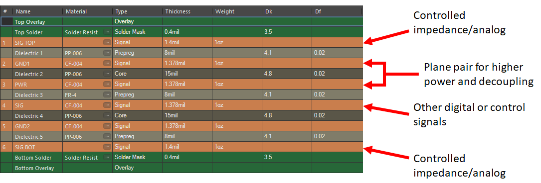
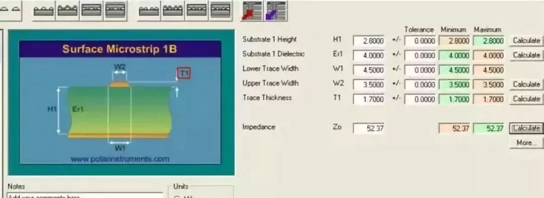
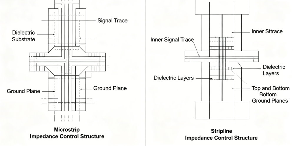
Characteristic impedance depends on the transmission line geometry, including trace width, thickness, height above the reference plane, and the dielectric constant of the substrate. In microstrip configurations, common for single-layer home PCBs, the top trace over a ground plane exposes part of the field to air, affecting the effective dielectric constant. Stripline, with traces sandwiched between planes, offers better control but requires multi-layer boards harder to fabricate at home. The formula for microstrip impedance, as detailed in IPC-2221, balances these factors to target values like 50 ohms for most RF work.
Dielectric materials like FR4 have a relative permittivity around 4.0 to 4.5, influencing impedance calculations. Trace etching precision at home impacts width tolerance, which directly alters impedance by several ohms. Copper thickness, typically 1 ounce (35 microns) in hobbyist blanks, also plays a role in skin effect at high frequencies. Understanding these principles allows hobbyists to predict and adjust for DIY high-frequency circuits.
Frequency dependence adds complexity; at gigahertz levels, losses increase, but for simple RF projects under 1 GHz, basic models suffice. Reflections occur when impedance changes abruptly, quantified by the reflection coefficient. Proper design minimizes voltage standing wave ratio (VSWR), vital for antenna performance.
Practical Solutions for Home PCB Fabrication
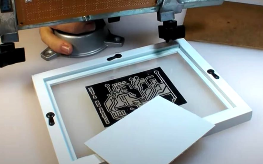
Start with a standard 1.6 mm thick FR4 substrate, pre-sensitized for etching, as it’s widely available and suitable for impedance control for hobbyists. Design traces using microstrip for simplicity: wider traces lower impedance, narrower ones raise it. Use online calculators to solve for width given your stackup—input height, copper weight, and Er to get precise dimensions before printing the mask. Print on glossy paper with a laser printer, transfer to the board via toner method, and etch with ferric chloride for clean edges.
Maintain consistent ground plane coverage under traces to stabilize the reference. For building impedance controlled PCBs at home, route signals away from edges where fringing fields distort impedance. Solder a solid ground plane on the bottom using copper tape if needed for prototypes. Test basic continuity and shorts before populating.
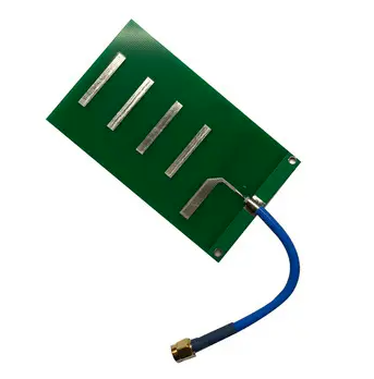
For impedance matching for antennas, design a 50-ohm feedline tapering to the antenna element. Simple RF projects like a dipole or patch antenna benefit from matched traces connecting to the driver stage. Avoid vias in critical paths as they introduce discontinuities; use top-layer routing where possible.
Related Reading: A Simple Guide to PCB Impedance Control for Hobbyists
Best Practices and Troubleshooting for DIY Projects
Adhere to manufacturing tolerances by over-etching slightly and measuring trace widths with calipers post-fabrication. Clean etchant residue thoroughly to prevent corrosion affecting long-term impedance. For multi-layer attempts, align prepregs carefully, but stick to two-layer for most simple RF projects.
Common issues include under-etching narrowing traces, raising impedance unexpectedly. Verify by comparing eye diagrams on an oscilloscope if available, or listen for signal strength in wireless tests. Adjust future designs iteratively based on performance.
Incorporate IPC-2141A test structures if space allows, like T-resonators for basic characterization without fancy gear. Ground stitching vias around traces reduce slotline modes. These practices elevate your impedance control for hobbyists game significantly.
Related Reading: Simplify PCB Impedance Control for Hobbyists: Easy Steps and Tips
Case Study: Simple RF Transmitter PCB
Consider a basic 433 MHz transmitter module PCB, a popular simple RF project. The design features a 50-ohm trace from oscillator to antenna pad, calculated for microstrip on FR4. Hobbyists etched prototypes, noting improved range after matching versus unmatched versions. Troubleshooting revealed ground plane gaps causing 10–15% impedance rise, fixed by filling with copper pours. This real-world example shows how impedance control transforms DIY high-frequency circuits from unreliable hacks to functional builds.
Conclusion
Mastering impedance control empowers electronic hobbyists to tackle DIY high-frequency circuits confidently. From understanding principles to practical etching and testing, these steps enable building impedance controlled PCBs at home without advanced facilities. Focus on microstrip designs, precise calculations, and iterative verification for success in simple RF projects and impedance matching for antennas. Consistent application yields better signal integrity and project outcomes. Experiment safely, and watch your homebrew RF gear perform reliably.
FAQs
Q1: What is the easiest way for hobbyists to achieve impedance control for hobbyists on single-layer PCBs?
A1: Microstrip traces on FR4 substrates provide a simple starting point for DIY high-frequency circuits. Calculate trace width using standard formulas or calculators based on board thickness and copper weight to target 50 ohms. Etch carefully to maintain dimensions, and ensure a full ground plane underneath. This approach suits building impedance controlled PCBs at home without multi-layer complexity. Test performance through basic RF output measurements.
Q2: How does impedance matching for antennas improve simple RF projects?
A2: Proper matching minimizes reflections, maximizing power transfer to the antenna in DIY high-frequency circuits. Design feedlines with consistent 50-ohm impedance to the radiator element. Hobbyists see range boosts and cleaner signals post-matching. Avoid abrupt width changes; use gradual tapers if needed. This is key for effective wireless prototypes.
Q3: Can hobbyists verify impedance on home-etched PCBs without professional tools?
A3: Use a NanoVNA or basic oscilloscope to observe reflections or eye patterns in impedance control for hobbyists setups. Compare signal quality before and after suspected mismatches. Iterative redesign based on range tests in simple RF projects works well. While not precise, these methods guide improvements effectively.
Q4: What common mistakes occur in building impedance controlled PCBs at home?
A4: Inconsistent etching leads to width variations altering impedance in DIY high-frequency circuits. Incomplete ground planes or via stubs introduce discontinuities. Overlooking dielectric inconsistencies in FR4 batches affects calculations. Address by measuring post-etch and refining masks. Following IPC-2221 guidelines prevents most issues.
References
IPC-2141A — Design Guide for High-Speed Controlled Impedance Circuit Boards. IPC
IPC-2221C — Generic Standard on Printed Board Design. IPC
IPC-6012E — Qualification and Performance Specification for Rigid Printed Boards. IPC, 2017