ALLPCB


Introduction
In high-speed electronics, the choice of dielectric materials in PCB layer stacks plays a critical role in signal integrity and overall system performance. Low Dk PCB stackups, which utilize materials with a low dielectric constant, minimize signal propagation delays and losses, making them essential for applications like RF circuits, high-frequency data transmission, and advanced computing. Engineers often face the challenge of achieving controlled impedance stackups while keeping manufacturing costs in check. This article explores how to design low Dk PCB stackups that optimize both performance metrics and PCB design cost optimization strategies. By understanding the interplay between material properties, layer arrangement, and impedance control, designers can create robust boards that meet stringent electrical requirements. The focus here is on practical engineering approaches grounded in established principles.
What Is a Low Dk PCB Stackup and Why It Matters
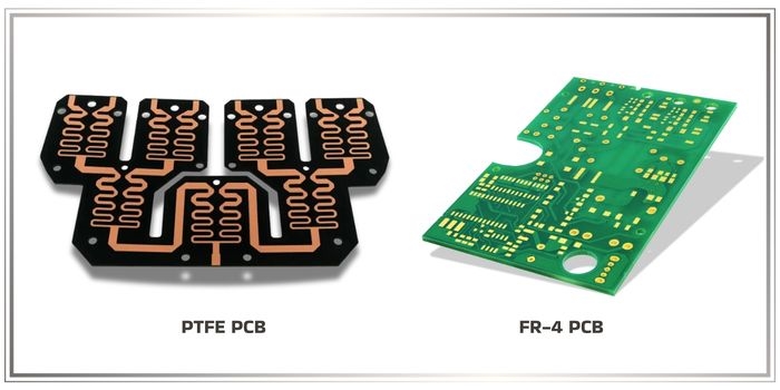
A low Dk PCB stackup refers to the vertical arrangement of conductive layers, dielectrics, and planes where the core and prepreg materials exhibit a dielectric constant (Dk) typically below 3.5. This contrasts with standard FR-4 materials, which have Dk values around 4.0 to 4.5, leading to higher signal attenuation at gigahertz frequencies. In a PCB layer stack, low Dk materials reduce the effective capacitance between traces, enabling faster signal rise times and lower insertion loss. For electric engineers working on impedance control PCBs, this becomes crucial in maintaining characteristic impedance, such as 50 ohms for single-ended lines or 100 ohms for differential pairs.
The relevance of low Dk PCB stackups intensifies in modern designs driven by 5G, automotive radar, and server backplanes, where signal speeds exceed 10 Gbps. Without proper stackup planning, mismatches in impedance can cause reflections, crosstalk, and electromagnetic interference, degrading performance. Cost considerations arise because low Dk materials are pricier than standard laminates, yet strategic stackup design allows PCB design cost optimization by reducing layer count or simplifying fabrication. Engineers must weigh these factors to balance speed, reliability, and budget in controlled impedance stackups.
Technical Principles of Low Dk Materials in PCB Stackups
The dielectric constant directly influences the speed of signal propagation in a PCB layer stack, governed by the formula for phase velocity: v = c / sqrt(Dk_eff), where c is the speed of light and Dk_eff is the effective dielectric constant. Low Dk materials, often thermoset resins reinforced with low-loss glass fibers, achieve Dk values as low as 2.5 to 3.2, allowing signals to travel closer to the speed of light in vacuum. This reduces skew between signals on different layers and minimizes dielectric losses, which are proportional to Dk * tan δ (loss tangent). In multilayer boards, the stackup configuration—alternating signal, ground, and power planes—affects Dk_eff, as fields fringe into adjacent dielectrics.
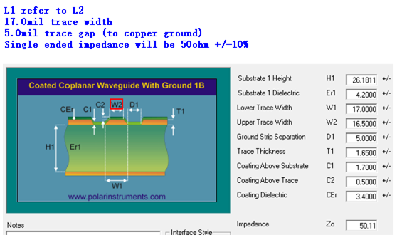
Impedance in controlled impedance stackups is calculated using models like the stripline or microstrip equations, where Z0 ≈ (87 / sqrt(Dk + 1.41)) * ln(5.98h / (0.8w + t)) for microstrips, with h as dielectric height, w as trace width, and t as copper thickness. Low Dk values permit wider traces for the same impedance, easing fabrication tolerances and reducing skin effect losses at high frequencies. However, thermal expansion differences between low Dk cores and standard prepregs can induce stresses, potentially leading to warpage if not managed.
Adherence to IPC-2221B design standards ensures that stackups account for these interactions, specifying guidelines for material selection and layer symmetry to maintain mechanical integrity. Variations in Dk with frequency and temperature further complicate designs, as Dk typically decreases slightly above 1 GHz but rises with humidity absorption.
Related Reading: Prepreg Thickness & Dielectric Constant: Optimizing PCB Performance
Designing Controlled Impedance Stackups with Low Dk Materials
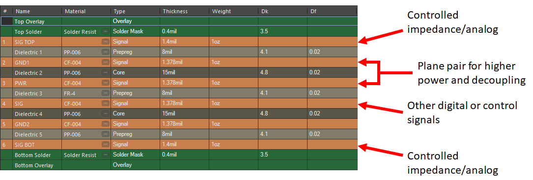
Effective low Dk PCB stackup design begins with defining impedance requirements based on the fastest signals and routing layers. Engineers typically use symmetric stackups with ground planes adjacent to signal layers to provide return paths and shield crosstalk, achieving broadband impedance control. For a 50-ohm microstrip, a low Dk prepreg thickness of 0.1 mm might require a trace width of 0.15 mm, compared to 0.12 mm on higher Dk materials, offering routing flexibility.
Layer sequencing prioritizes high-speed signals on outer layers or next to planes, with power distribution cores placed centrally for stability. Hybrid stackups blend low Dk materials for RF sections with cost-effective FR-4 for low-speed areas, optimizing the overall PCB layer stack. Prepreg selection is key; low Dk sheets with low resin content ensure uniform Dk_eff across the board.
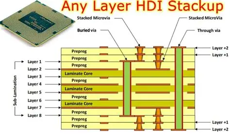
Fabrication aspects include controlling copper foil roughness, as low-profile foils reduce conductor losses in high-frequency low Dk environments. Sequential lamination processes may be necessary for thick stackups to avoid via stub effects, aligning with J-STD-001 requirements for soldering reliability.
Related Reading: Understanding Dielectric Constant: A Beginner's Guide to Rogers PCB Materials
Balancing Performance and Cost in Low Dk PCB Stackups
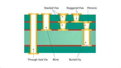
PCB design cost optimization in low Dk stackups involves minimizing material volume while preserving electrical performance. Using thinner cores and prepregs reduces raw material costs, but engineers must verify via reliability under thermal cycling. Fewer layers through dense routing—enabled by low Dk's wider traces—cut drilling and plating expenses, though blind or buried vias add complexity.
Material hybridization offers a practical trade-off: low Dk for 20-30% of the stackup in critical zones, with standard materials elsewhere. This approach maintains controlled impedance stackup integrity without full premium material adoption. Supplier qualification ensures Dk consistency, as batch variations can shift impedance by 5-10%.
Mechanical stability demands symmetric builds around the neutral axis, preventing bow and twist per IPC-6012DS specifications for high-density interconnects. Panel utilization during manufacturing further optimizes costs by nesting multiple boards efficiently.
Best Practices and Common Pitfalls in Low Dk Stackup Design
Start with simulation tools to model stackup impedance across frequencies, iterating on dielectric thicknesses until tolerances meet ±10% specs. Always incorporate power-ground plane pairs to decouple noise, enhancing signal integrity in impedance control PCBs. Validate designs with time-domain reflectometry (TDR) measurements post-prototype.
Pitfalls include overlooking Df (dissipation factor), where high Df negates low Dk benefits through increased attenuation. Thermal management is vital; low Dk materials often have lower Tg, risking delamination in reflow. Cost overruns stem from over-specifying low Dk everywhere—assess signal speed needs layer-by-layer.
Document the stackup drawing meticulously, including material callouts and press cycles, to ensure reproducibility.
Conclusion
Low Dk PCB stackups enable superior high-speed performance through reduced dielectric losses and precise impedance control, while thoughtful design choices drive PCB design cost optimization. Engineers achieve this by hybrid material strategies, symmetric layer arrangements, and adherence to standards like IPC-2221B and IPC-6012DS. Balancing trace geometries, plane proximity, and fabrication feasibility yields reliable controlled impedance stackups. As frequencies rise, mastering these principles will define successful PCB layer stack designs. Prioritize simulation, validation, and cost-aware material selection for optimal outcomes.
FAQs
Q1: What factors most influence impedance in a low Dk PCB stackup?
A1: Impedance depends on dielectric thickness, Dk value, trace width, and copper thickness in the PCB layer stack. Low Dk materials allow wider traces for the same Z0, improving manufacturability. Ground plane proximity controls field distribution, essential for controlled impedance stackups. Simulations refine these parameters to ±5-10% accuracy.
Q2: How does low Dk affect PCB design cost optimization?
A2: Low Dk materials raise material costs but enable fewer layers via better routing density, offsetting expenses. Hybrid stackups use premium dielectrics selectively for high-speed sections. Thinner prepregs reduce volume, and efficient panelization lowers fabrication costs. Overall, strategic low Dk PCB stackup design balances performance gains with savings.
Q3: Why is layer symmetry important in impedance control PCBs?
A3: Symmetry around the neutral axis minimizes warpage from CTE mismatches in low Dk stackups. It ensures uniform via plating and maintains impedance consistency across layers. Asymmetric builds risk reliability failures under thermal stress. Standards like IPC-6012DS guide symmetric configurations for high-reliability boards.
Q4: Can standard materials complement low Dk in a controlled impedance stackup?
A4: Yes, hybrid approaches place low Dk cores for RF signals and FR-4 for DC/power layers. This optimizes cost without compromising impedance control PCB performance. Careful prepreg matching prevents Dk_eff discontinuities at interfaces. Testing verifies signal integrity across transitions.
References
IPC-2221B — Generic Standard on Printed Board Design. IPC, 2003
IPC-6012DS — Qualification and Performance Specification for High Density Interconnect (HDI) Printed Boards. IPC, 2015
J-STD-001H — Requirements for Soldered Electrical and Electronic Assemblies. IPC, 2020