 ALLPCB


Introduction
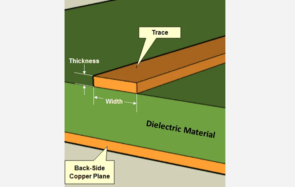
Trace clearance refers to the minimum distance maintained between conductive elements on a printed circuit board, such as traces, pads, and vias. In PCB manufacturing, insufficient clearance often leads to defects that compromise board reliability and drive up production costs. Engineers must prioritize this parameter during design to align with fabrication capabilities and avoid rework. Violations can manifest during etching, plating, or solder mask application, resulting in shorts or arcing under operational stress. Understanding the interplay between design intent and manufacturing tolerances is essential for cost optimization. This article explores trace clearance principles, common pitfalls, and DFM strategies tailored for electric engineers.
What Is Trace Clearance and Why It Matters in PCB Manufacturing
Trace clearance is the air gap or insulating distance between adjacent copper features on a PCB, critical for preventing unintended electrical connections. In the PCB fabrication process, this spacing ensures reliable etching and plating without bridging. Manufacturers specify minimum clearances based on their equipment tolerances, typically tighter for high-density boards. Neglecting these can cause PCB manufacturing defects like copper slivers or insufficient isolation, leading to field failures. From a factory perspective, adhering to DFM guidelines reduces scrap rates and accelerates time-to-market. Ultimately, proper clearance supports higher yields and cost optimization across production volumes.
Technical Principles Behind Trace Clearance in the PCB Fabrication Process
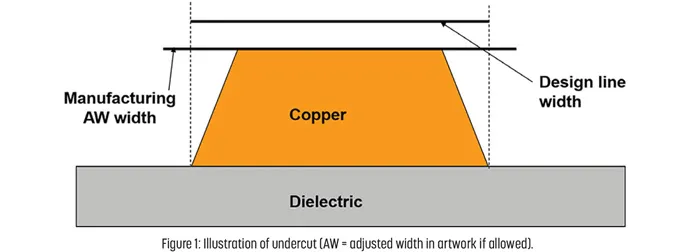
During PCB fabrication, trace clearance must account for etching undercuts, where chemical processes erode copper laterally. This phenomenon, governed by the etch factor, reduces effective spacing if designs push limits. Plating steps, such as electroless copper deposition, can also encroach on clearances if vias or traces are too close. Solder mask application requires adequate gaps to prevent bridging or voids that expose copper. Environmental factors like humidity influence creepage distances over surfaces. Standards like IPC-2221 provide generic guidelines for spacing based on voltage and board location, helping engineers predict manufacturing outcomes.
Multilayer boards introduce additional challenges, as inner layer alignments depend on lamination pressures and drill registration. Misregistration during imaging can shrink clearances unexpectedly. Factory-driven insights emphasize verifying stackup effects on trace-to-trace distances. Thermal expansion during soldering further stresses tight clearances, potentially causing delamination. Engineers should model these interactions early to avoid trace clearance violations.
Common Trace Clearance Violations and Associated PCB Manufacturing Defects
Trace clearance violations often stem from designs ignoring fab house capabilities, leading to shorts during production. In etching, overly tight spacing traps etchant, causing acid traps or mouse bites that bridge traces. Copper slivers from poor etching control can float and create intermittent contacts post-fabrication. During panel plating, violations exacerbate uneven deposition, resulting in whiskers that short circuits. These PCB manufacturing defects not only lower yields but also trigger costly inspections and respins.
Solder mask misalignment amplifies issues in high-density interconnects, where thin masks fail to cover edges adequately. Post-bake warpage can pull traces closer, violating designed clearances. Factories report higher defect rates in fine-pitch designs without DFM review. Arcing risks emerge in high-voltage applications if clearances fall below thresholds. Addressing these proactively prevents escalation to assembly failures.
DFM Best Practices for Trace Clearance and Cost Optimization
Design for Manufacturability (DFM) starts with selecting clearances compatible with the chosen fab process, such as 5-mil minimums for standard panels. Engineers should request fab DFM reports early to flag potential violations. Use annular ring controls around vias to maintain drill-to-copper distances, preventing breakout defects. Balance copper distribution across layers to minimize plating variances that erode clearances. Incorporate test coupons for clearance verification during qualification per IPC-6012.
Optimize routing by grouping signals with similar voltages, reducing high-to-low potential spans. Factory insights recommend 3W rule approximations for signal integrity alongside clearance rules. Simulate etch compensation in design tools to predict final dimensions. For cost optimization, avoid exotic processes like fine-line imaging unless volume justifies premiums. Regular fab audits ensure consistent adherence to these practices.
Troubleshooting Trace Clearance Issues in Production
When trace clearance violations appear in incoming inspections, first review Gerber data against fab specs. Microsection analysis reveals etch undercuts or plating buildup as root causes. Adjust panelization to improve uniformity in multi-up arrays. If defects persist, widen clearances iteratively while monitoring impedance. Factories use automated optical inspection (AOI) to catch bridges early, saving rework costs.
For recurring issues, correlate with material types, as higher Tg laminates resist warpage better. Collaborate with suppliers on process windows for imaging and developing. Post-troubleshooting, update design libraries with validated clearances. IPC-A-600 criteria guide acceptability judgments during these reviews. This systematic approach minimizes downtime and enhances future yields.
Conclusion
Maintaining proper trace clearance is foundational to robust PCB manufacturing, directly impacting defect rates and costs. By integrating DFM from design onset, engineers sidestep common pitfalls like etching bridges and plating shorts. Standards-aligned practices ensure compliance across the fabrication process. Proactive verification and troubleshooting further optimize outcomes. Ultimately, these strategies deliver reliable boards at lower total cost, empowering electric engineers to focus on innovation.
FAQs
Q1: What are the main PCB manufacturing defects caused by trace clearance violations?
A1: Trace clearance violations frequently lead to shorts, copper bridging, and slivers during etching in the PCB fabrication process. These defects reduce yields and necessitate costly respins. Factories mitigate them through DFM checks and process controls. Proper spacing per standards prevents arcing and signal integrity issues.
Q2: How does DFM help avoid trace clearance violations?
A2: DFM guidelines ensure designs match fab capabilities, specifying minimum clearances to counter etching undercuts and plating variances. Engineers receive feedback on potential violations before production. This approach optimizes costs by minimizing scrap and rework. Factory-driven DFM promotes balanced copper distribution for uniform processing.
Q3: Why is trace clearance critical in the PCB fabrication process?
A3: In PCB fabrication, trace clearance prevents defects like acid traps and mask bridging, ensuring electrical isolation. Tolerances during imaging and developing demand conservative designs. Violations inflate costs through lower yields and failures. Standards like IPC-2221 guide voltage-based spacing for reliability.
Q4: How can engineers optimize costs related to trace clearance in manufacturing?
A4: Cost optimization involves selecting fab-appropriate clearances and using etch compensation. DFM reviews flag risks early, avoiding expensive prototypes. Verify with coupons and AOI for high-volume runs. Balanced designs reduce plating inconsistencies, enhancing throughput.
References
IPC-2221B — Generic Standard on Printed Board Design. IPC, 2003
IPC-6012E — Qualification and Performance Specification for Rigid Printed Boards. IPC, 2017
IPC-A-600K — Acceptability of Printed Boards. IPC, 2020


