What's the Deal with Controlled Impedance in PCB Design?
Master controlled impedance in PCB design to ensure signal integrity for high-speed circuits. Learn how to prevent signal distortion and reduce EMI.
Learn why copper weight is crucial in PCB layout thermal design. Optimize heat dissipation and reliability with expert tips from ALLPCB!
Explore via-in-pad current capacity in PCBs. Learn about trace width, thermal resistance, and high-current design tips in this detailed guide.
A step-by-step guide on aligning PCB layout with plastic enclosure design. Explore ECAD–MCAD collaboration, mold engineering tips, and prototyping methods to avoid costly rework.
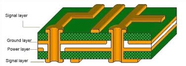
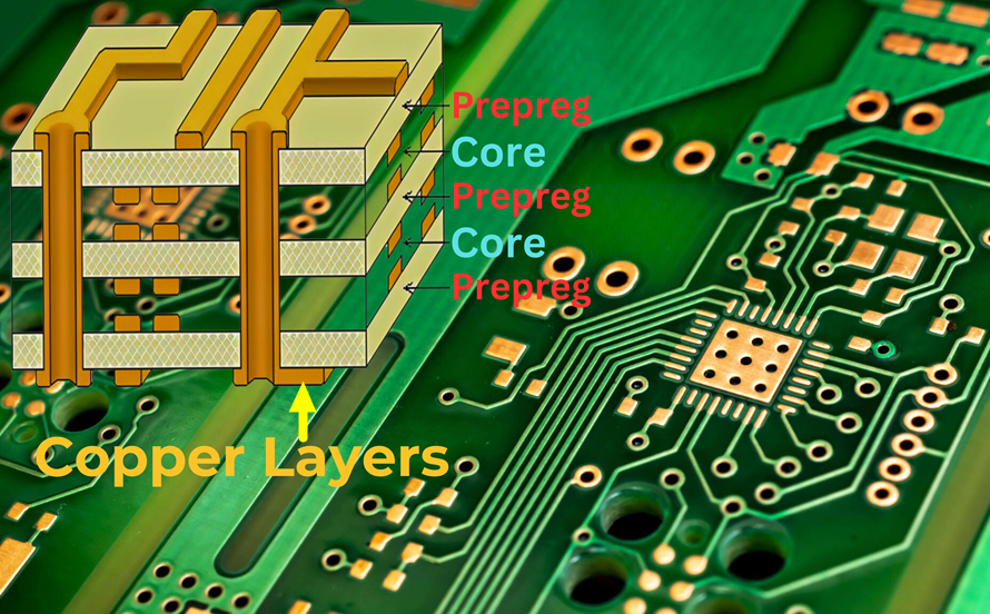
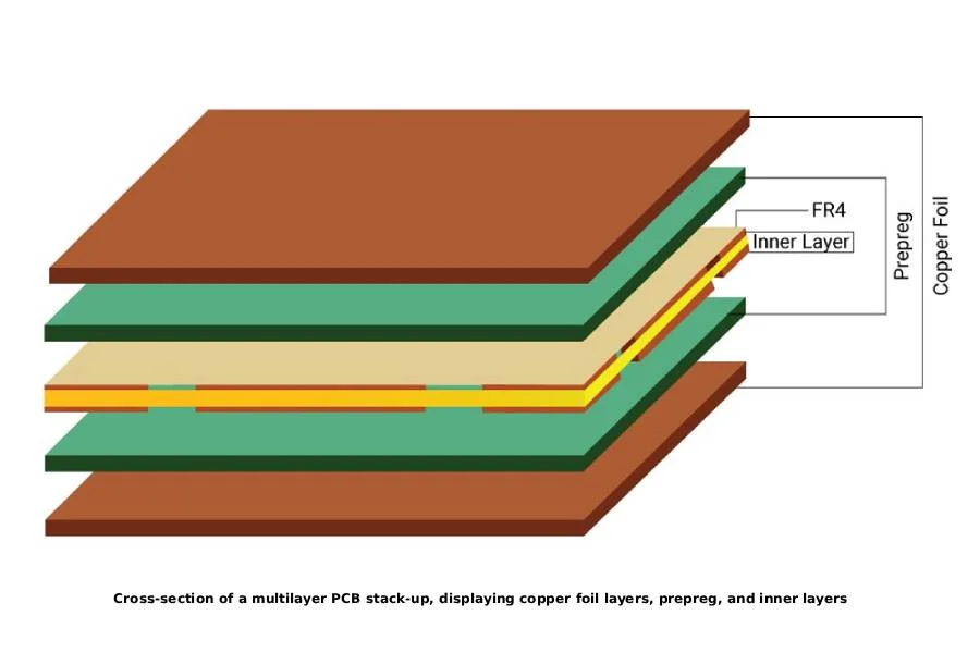
Explore PCB stackup design for power electronics, focusing on high-current handling, thermal management, and minimizing voltage drop.
Learn how to prevent solder wicking in via-in-pad assembly with tips on solder paste, stencil design, and reflow profiles for SMT success.
Master high-frequency PCB stack-up design with our ultimate guide on layer stacks, impedance control, microstrip vs. stripline, and more.
Learn PCB stackup design guidelines for analog, digital, and mixed-signal circuits. Master noise isolation and signal integrity with expert tips.
Master easy PCB impedance control with our guide for hobbyists. Learn simple steps & practical tips to improve signal quality in high-speed designs.
Learn about Power Distribution Network (PDN) via placement for low impedance power delivery and EMI reduction in PCB design with expert tips.
Learn via placement for PCB design with this beginner's guide on via sizes, types, and spacing. Master the basics for better layouts!
Master copper pour design rules for PCB layout with this guide on clearances, spacing, and signal integrity for optimal performance.
Explore microstrip vs stripline for PCB impedance control. Compare features, benefits, and applications in this detailed guide by ALLPCB.
Explore high-frequency PCB material selection with a deep dive into Dk and Df. Learn about low loss tangent, Rogers vs FR4, and PTFE design.
Learn the art of via placement for optimal PCB routing and signal flow. Get tips on effective via use and design for better performance.
Explore the complete PCB impedance control workflow from design to manufacturing. Learn key steps for signal integrity in high-speed designs.
Learn practical layout techniques to minimize EMI in high-frequency PCBs, including grounding, shielding, and decoupling capacitor strategies.
Explore solid vs. hatched copper pour fill types in PCB design. Learn their benefits, applications, and best practices for optimal performance.
Uncover outdated EMC design guidelines to avoid in PCB design. Learn better practices for interference-free, compliant boards with ALLPCB!
Explore the pros and cons of 4-layer, 6-layer, and 8-layer PCB stackups for high-speed design. Choose the best configuration for your project!