 ALLPCB


Introduction
Thermal pad design plays a critical role in surface mount technology (SMT) assembly, ensuring effective heat dissipation and reliable solder joints for high-power components. As electronic devices become smaller and more complex, challenges in SMT thermal pad alignment, solder paste application, reflow soldering, and thermal pad rework have grown. These issues often lead to SMT assembly defects like voiding, insufficient wetting, and component misalignment. For electrical engineers, addressing these manufacturing hurdles is vital to maintaining product reliability and performance. This article explores the technical principles behind thermal pad design, identifies common challenges in SMT assembly, and provides practical solutions aligned with industry standards. By understanding these aspects, engineers can optimize their processes and reduce defects in production.
What Are Thermal Pads in SMT Assembly and Why Do They Matter
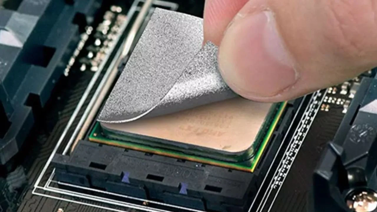
Thermal pads are specialized areas on a printed circuit board (PCB) designed to transfer heat away from components, often integrated into packages like quad flat no-lead (QFN) or dual flat no-lead (DFN). These pads, typically located beneath the component, connect to the PCB through solder joints, aiding in thermal management and sometimes providing electrical grounding. Their importance lies in preventing overheating, which can degrade component performance or cause failure in high-power applications such as power amplifiers or LED drivers.
Effective thermal pad design directly impacts SMT assembly quality. Poor design or implementation can result in uneven heat distribution, weak solder connections, or mechanical stress during reflow soldering. For electrical engineers, understanding thermal pad functionality is essential to achieving reliable assemblies and meeting stringent performance requirements in modern electronics.
Technical Principles of Thermal Pad Design in SMT Assembly
Thermal pads must balance heat dissipation with solder joint integrity. The design involves several key principles governed by industry standards to ensure functionality. First, the pad size and shape should match the component footprint, providing sufficient area for heat transfer while avoiding excessive solder volume that could lead to defects like bridging. Standards such as IPC-7351B provide guidelines for land pattern design, ensuring compatibility between component and PCB layouts.
Another principle is thermal via placement. Vias under the pad connect to inner or bottom copper layers, enhancing heat dissipation. However, improper via design can trap air or flux during reflow soldering, causing voids. JEDEC J-STD-020E outlines moisture sensitivity and reflow profiles to mitigate such risks during assembly.
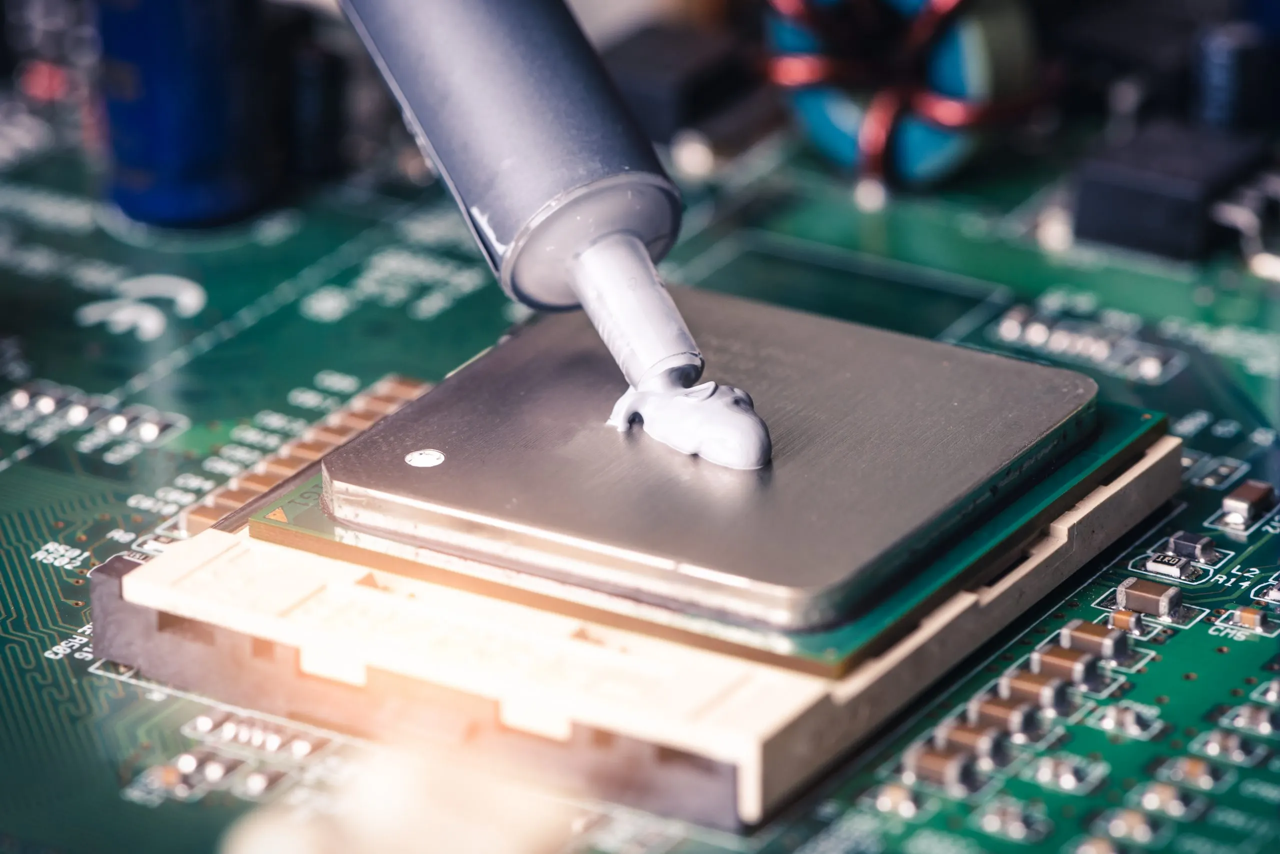
Finally, solder paste application on thermal pads requires precision. Too much paste can cause floating or misalignment, while too little may result in insufficient wetting. The stencil design, often guided by IPC-7525B, must account for paste volume to achieve uniform coverage. These principles form the foundation for addressing manufacturing challenges in SMT assembly.
Common Manufacturing Challenges with Thermal Pads in SMT Assembly
SMT Thermal Pad Alignment Issues
Misalignment between the thermal pad and component during placement is a frequent challenge. This often occurs due to inaccuracies in pick-and-place machines or discrepancies in PCB fabrication tolerances. Misaligned pads can lead to uneven solder distribution, reducing thermal efficiency and causing mechanical stress. Adhering to IPC-A-600K for PCB acceptability ensures dimensional accuracy, minimizing alignment errors.
Solder Paste Application on Thermal Pads
Applying solder paste to thermal pads is complex due to the large surface area. Uneven paste deposition or incorrect stencil aperture design can result in insufficient solder or excess flux residue. This affects joint quality and may cause SMT assembly defects like voiding. IPC-7525B provides stencil design guidelines to optimize paste transfer for consistent results.
Reflow Soldering Challenges with Thermal Pads
During reflow soldering, thermal pads face risks such as tombstoning or solder balling due to uneven heating. Large pads often require more heat, which can overstress surrounding components if the reflow profile is not optimized. JEDEC J-STD-020E specifies reflow temperature profiles to balance heat distribution and prevent defects during this critical stage.
Thermal Pad Rework Difficulties
Reworking thermal pads after assembly poses unique challenges. Removing and replacing components without damaging the pad or surrounding traces requires precise heat control. Excessive heat can cause pad lift or delamination, while insufficient heat may leave solder residue. Guidelines from IPC-7711/7721C offer best practices for rework and repair to maintain PCB integrity.
Practical Solutions for Thermal Pad Design and Assembly Challenges
Optimizing SMT Thermal Pad Alignment
To ensure accurate alignment, engineers should verify component footprints against PCB layouts using design rules from IPC-7351B. Implementing fiducial markers near thermal pads can enhance placement precision during assembly. Additionally, regular calibration of pick-and-place equipment minimizes mechanical errors, reducing misalignment risks.
Improving Solder Paste Application for Thermal Pads
Effective solder paste application starts with proper stencil design. Apertures should be segmented into smaller openings, often in a grid pattern, to control paste volume and prevent excess deposition. Following IPC-7525B, a 50 to 80 percent area ratio for apertures ensures balanced coverage. Using a no-clean flux paste also reduces residue buildup under components.
Enhancing Reflow Soldering for Thermal Pads
Optimizing the reflow soldering process involves tailoring the temperature profile to the thermal mass of the pad and component. A gradual preheat stage, as recommended by JEDEC J-STD-020E, prevents thermal shock. Additionally, nitrogen atmospheres during reflow can reduce oxidation, improving solder wetting on large thermal pads and minimizing defects.
Streamlining Thermal Pad Rework Processes
For rework, using localized heating tools like hot air stations with controlled temperature settings prevents damage to adjacent areas. Preheating the PCB to around 100 degrees Celsius before applying focused heat, as suggested by IPC-7711/7721C, ensures safe component removal. Cleaning pads with isopropyl alcohol and a brush removes residual flux without harming the board.
Preventing SMT Assembly Defects
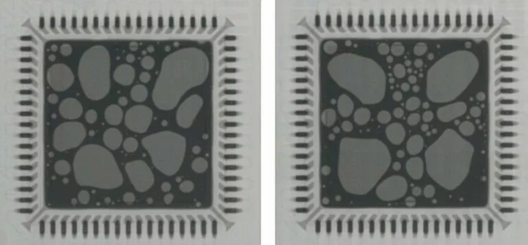
Proactive measures can significantly reduce SMT assembly defects related to thermal pads. Regular inspection using X-ray imaging detects voids or insufficient solder under pads. Automated optical inspection systems also identify misalignment or paste issues before reflow. Adhering to IPC-A-610H for acceptability criteria ensures assemblies meet quality standards.
Troubleshooting Insights for Thermal Pad Assembly Issues
When defects occur, systematic troubleshooting is essential. If voiding appears under thermal pads during X-ray inspection, review the reflow profile against JEDEC J-STD-020E guidelines to ensure proper outgassing of flux. Insufficient wetting often indicates inadequate paste volume or poor stencil design, which can be corrected using IPC-7525B recommendations. For misalignment issues, check PCB tolerances against IPC-A-600K standards and adjust placement parameters accordingly. Documenting each issue and solution builds a knowledge base for future assemblies, enhancing process reliability.
Conclusion
Thermal pad design in SMT assembly is a cornerstone of reliable electronic manufacturing, directly influencing heat management and solder joint quality. Challenges like SMT thermal pad alignment, solder paste application, reflow soldering issues, and thermal pad rework can disrupt production if not addressed. By applying practical solutions grounded in industry standards such as IPC and JEDEC, electrical engineers can overcome these hurdles. From optimizing stencil designs to fine-tuning reflow profiles, each step contributes to minimizing SMT assembly defects. A focus on precision and adherence to best practices ensures high-quality outcomes in modern electronics production.
FAQs
Q1: How can SMT thermal pad alignment issues be prevented during assembly?
A1: SMT thermal pad alignment issues can be minimized by using fiducial markers for precise placement and verifying footprints against IPC-7351B guidelines. Regular calibration of pick-and-place machines also ensures accuracy. Inspecting PCB dimensional tolerances as per IPC-A-600K before assembly helps identify potential discrepancies, allowing engineers to adjust designs or processes accordingly for consistent results.
Q2: What are the best practices for solder paste application on thermal pads?
A2: For effective solder paste application on thermal pads, use segmented stencil apertures with a 50 to 80 percent area ratio as per IPC-7525B. This controls paste volume and prevents excess deposition. Opt for no-clean flux paste to reduce residue. Ensure stencil cleanliness and alignment to achieve uniform coverage, avoiding defects like insufficient wetting or bridging.
Q3: How does reflow soldering impact thermal pad performance?
A3: Reflow soldering of thermal pads requires a balanced temperature profile to avoid defects like tombstoning or voiding. Following JEDEC J-STD-020E, a gradual preheat prevents thermal shock, while proper peak temperatures ensure solder wetting. Uneven heating can stress components, so nitrogen atmospheres may be used to enhance joint quality and thermal performance.
Q4: What techniques improve thermal pad rework without damaging the PCB?
A4: Thermal pad rework can be improved by preheating the PCB to about 100 degrees Celsius before using localized hot air tools, as guided by IPC-7711/7721C. Controlled heating prevents pad lift or trace damage. Clean pads with isopropyl alcohol post-rework to remove flux residue, ensuring the board remains intact for subsequent assembly steps.
IPC-7351B — Generic Requirements for Surface Mount Design and Land Pattern Standard. IPC, 2010.
IPC-7525B — Stencil Design Guidelines. IPC, 2012.
IPC-A-600K — Acceptability of Printed Boards. IPC, 2020.
IPC-A-610H — Acceptability of Electronic Assemblies. IPC, 2020.
IPC-7711/7721C — Rework, Modification and Repair of Electronic Assemblies. IPC, 2017.
JEDEC J-STD-020E — Moisture/Reflow Sensitivity Classification for Nonhermetic Surface Mount Devices. JEDEC, 2014.


