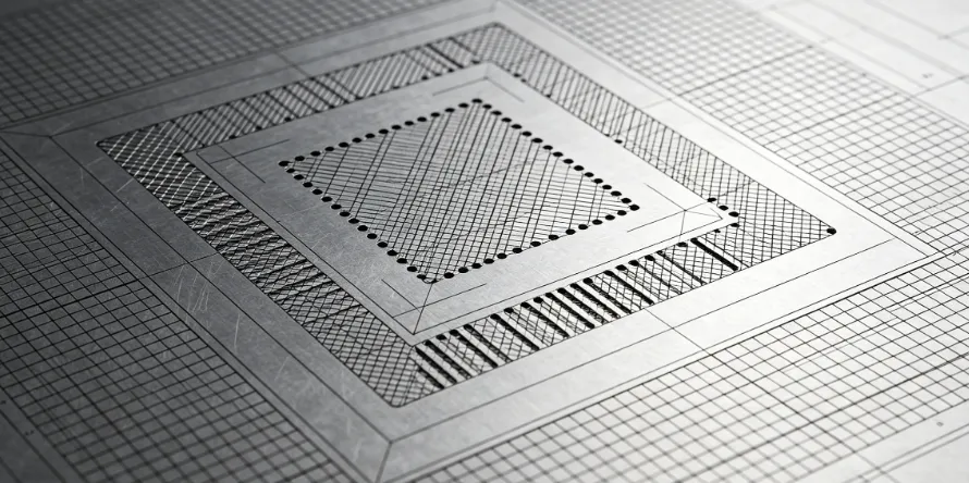
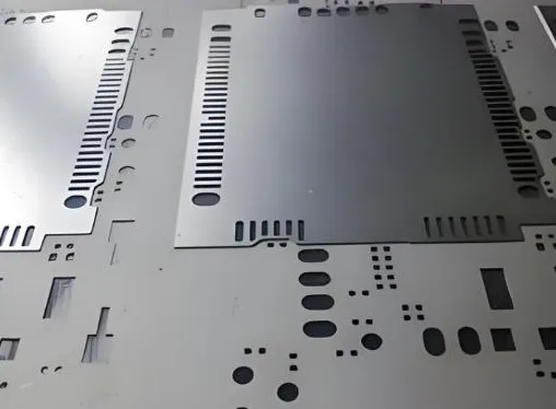
Stainless Steel Stencils: The Gold Standard for High Volume PCB Assembly
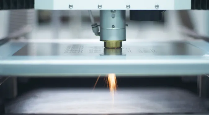
Stainless steel stencils provide durability and precision for high-volume PCB assembly. Learn about laser cut stencils and framed stencil best practices.
Framed vs frameless stencils: compare advantages, costs, and mounting systems to select the best solution for your PCB production volume.
Explore advanced aperture design techniques for laser cut stencils to improve paste release on BGA and QFN packages through modified aperture shapes.
Optimize your stencil aperture design to ensure reliable solder joints. Learn how area and aspect ratios prevent PCB defects like bridging and tombstoning for better assembly yields.
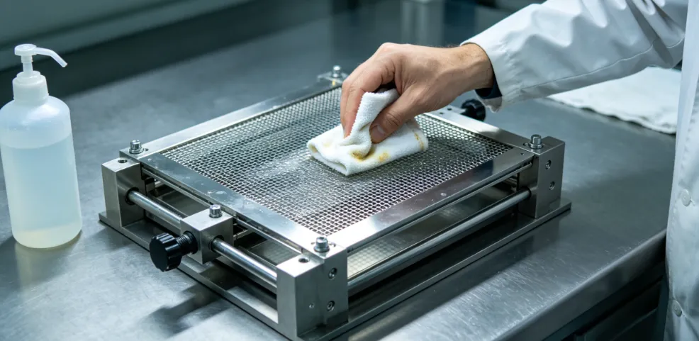
Improve your assembly yields with regular laser cut stencil maintenance. Follow expert cleaning and storage practices to prevent solder paste residue buildup and ensure precise joint quality.
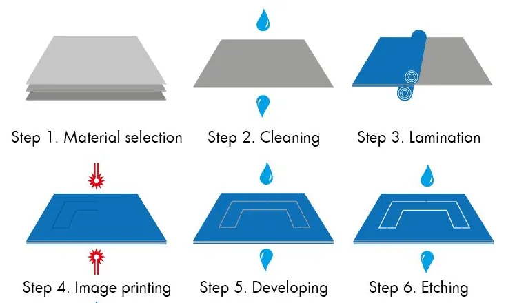
Find out if an etched SMT stencil suits your prototype project. Learn about chemical etched stencils and practical tips for low cost SMT stencil use.
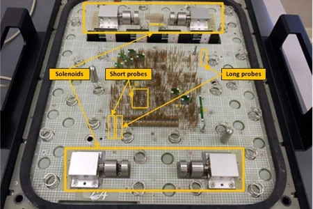
Optimize PCB manufacturing yields with design for in circuit testability. Strategic test point placement and layout optimization improve fault detection while reducing total production costs.
Stencil surface finish affects SMT solder paste release. Electropolishing and nano coatings reduce adhesion for improved transfer. This article covers mechanisms, selection, maintenance, and troubleshooting.
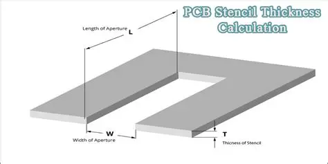
Stencil thickness directly affects the volume and consistency of solder paste deposited on circuit boards. This analysis explains the technical principles behind the process and offers practical advice on selecting the right thickness for reliable PCB assembly outcomes.
Follow these PCB stencil basics to choose the right foil thickness. Learn how to balance solder paste volume for fine pitch components to avoid bridging and ensure reliable joints on every build.
Compare stainless steel and nickel frameless stencil materials to optimize your PCB assembly process. Learn how material durability and aperture precision impact production costs and yield.
Secure your leaded assembly legal status using the RoHS exemption route. This article covers technical justifications and compliance strategies for high performance electronics manufacturing.
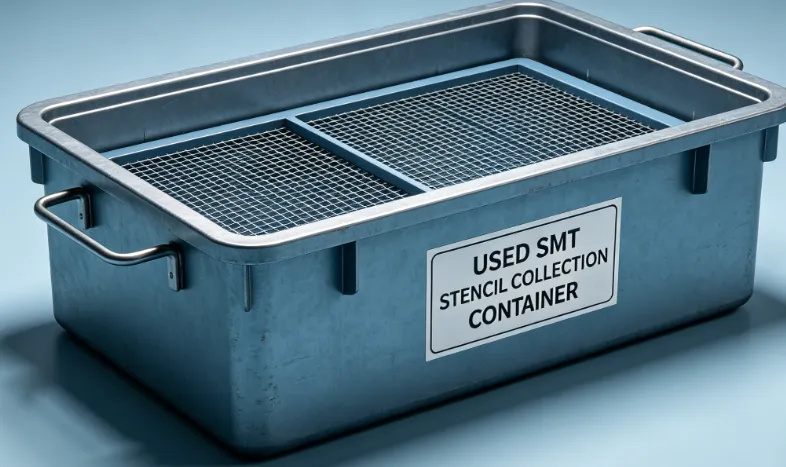
Implementing PCB stencil recycling helps manufacturers recover high grade metal and reduce landfill waste. Learn about the material recovery process and sustainable SMT stencil disposal practices.
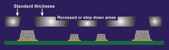
Step up stencils enhance PCB joint reliability by optimizing solder paste volume. Learn about aperture design and keep out areas to reduce manufacturing defects in mixed technology assemblies.
Properly match stencil thickness to your PCB layout for consistent solder paste deposition. Learn how pad geometries and component density ensure long term joint reliability in this guide.
Control in circuit testing expenses with expert cost analysis. Manage budgeting for ICT fixtures and programming while implementing efficient strategies to reduce your total PCB testing costs.
Identify and fix leaded assembly defects such as solder bridges and cold joints. Use our practical troubleshooting guide to improve PCB reliability and ensure high quality production results.
Improve your leaded assembly results by selecting the best flux for every project. Understand how different solder flux types ensure high solder joint quality for durable hobbyist electronics.
Achieve precise solder paste release by optimizing unmounted stencil aperture design. This expert guide covers area ratios and electro polishing to reduce PCB assembly defects and rework.