ALLPCB


Introduction
Mixed technology PCB design combines surface-mount technology components with through-hole components on the same board. This approach allows engineers to leverage the density and automation advantages of SMT while retaining the mechanical strength and reliability benefits of through-hole parts for specific applications such as connectors or high-power devices. The integration requires careful attention to assembly sequences, thermal profiles, and layout constraints to maintain manufacturability and long-term performance. Industry professionals often encounter this hybrid configuration in applications where not all required components are available in SMT packages or where mechanical robustness is essential. Proper planning from the schematic stage onward helps avoid common issues during soldering and inspection.
Why Mixed Technology PCB Design Matters
Hybrid PCB designs remain prevalent because they balance cost, performance, and availability constraints that pure SMT or pure through-hole boards cannot always satisfy. Through-hole components provide superior mechanical attachment for parts subject to vibration or physical stress, while SMT enables higher component density and smaller overall board sizes. Engineers must account for differing soldering requirements, as SMT typically undergoes reflow while through-hole parts often use wave or selective soldering. This dual-process reality influences everything from pad design to component orientation and board material selection. Adhering to established guidelines ensures the final assembly meets reliability targets across various operating environments.
Technical Principles of Mixed Assembly
The fundamental challenge in mixed technology boards arises from the sequential nature of the soldering processes. SMT components are placed and reflowed first to avoid exposing them to the higher temperatures and mechanical stresses of wave soldering. Through-hole components are then inserted and soldered, which may involve masking certain areas or using fixtures to protect already-mounted SMT parts. Thermal expansion differences between the board substrate and components can lead to warpage if not managed through proper stack-up design and support during processing. Solder joint formation also varies: reflow produces controlled fillet shapes on SMT pads, whereas wave soldering relies on capillary action through plated holes for through-hole leads.
Component placement strategies must separate the two technologies spatially where possible. Placing through-hole parts away from dense SMT areas reduces the risk of solder bridging or shadowing during wave soldering. Board warpage becomes a critical factor because uneven heating during reflow can distort the substrate, affecting subsequent through-hole insertion and alignment.
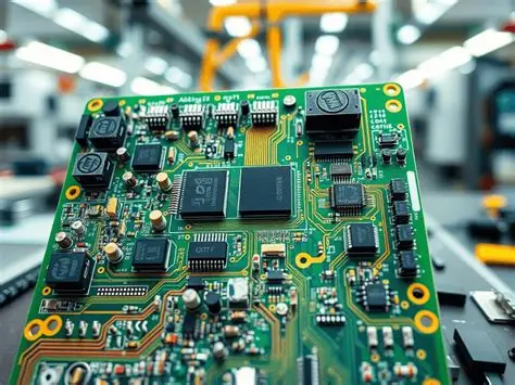
Design rules for pad and hole dimensions follow general principles outlined in relevant IPC documents to ensure adequate annular rings and solderability. Moisture sensitivity of components adds another layer of complexity, requiring controlled storage and baking procedures before assembly begins.
Best Practices for Component Placement and Process Flow
Effective mixed technology design begins with early collaboration between layout engineers and manufacturing teams. SMT components should occupy the primary side of the board, with through-hole parts positioned to allow straightforward insertion after reflow. Orientation of polarized through-hole components must align with assembly fixturing to prevent errors during automated or manual insertion. Keeping sufficient clearance between SMT pads and through-hole barrels minimizes the chance of solder defects when using wave processes.
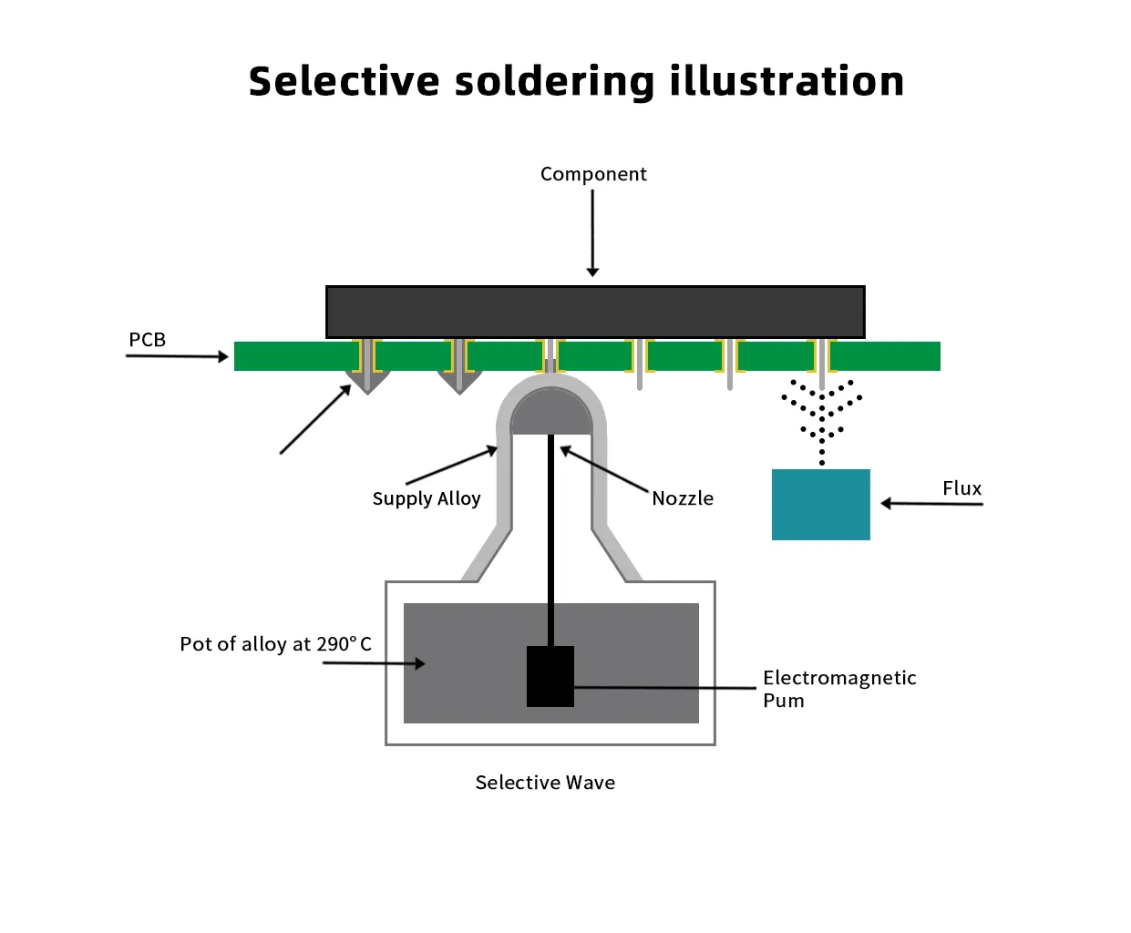
Engineers often employ selective soldering for boards with mixed populations to target only through-hole joints while protecting surrounding SMT areas. This technique reduces thermal exposure compared to full wave soldering and improves yield on densely populated boards. Stencil design for the SMT stage must avoid depositing paste into through-hole locations unless a paste-in-hole approach is intentionally used. Post-reflow inspection verifies SMT joint quality before through-hole assembly proceeds, allowing early detection of issues that could compound later.
Thermal profiling requires separate validation for each soldering step. The reflow profile must accommodate the most sensitive SMT components, while the subsequent through-hole process accounts for any additional heat sinking from already-attached parts. Board support fixtures during wave or selective soldering help control warpage and maintain planarity.
Following these steps aligns with established practices for reliable mixed assemblies and supports compliance with acceptance criteria in standards such as J-STD-001.
Additional Considerations for Reliability and Inspection
Reliability in hybrid boards depends on consistent solder joint quality across both technologies. Visual and automated optical inspection after each major process step catches defects before they propagate. X-ray inspection proves valuable for verifying through-hole fill and detecting voids hidden beneath SMT components. Cleaning processes must address residues from both reflow flux and wave soldering flux without damaging sensitive parts.
Material selection plays a supporting role, with laminates chosen for dimensional stability under multiple thermal cycles. Copper weight and trace routing around mixed areas should accommodate current-carrying needs without creating localized hot spots. Documentation of the complete process flow, including approved deviations, aids troubleshooting and supports traceability requirements in regulated industries.
Conclusion
Successful integration of through-hole and SMT components on a single PCB hinges on methodical layout planning, sequenced assembly processes, and adherence to proven engineering practices. By addressing placement constraints, thermal management, and process compatibility early in the design cycle, engineers achieve reliable performance without unnecessary complexity. Attention to industry-accepted guidelines helps ensure consistent quality from prototype through volume production. The hybrid approach continues to offer practical advantages when component requirements span both technologies.
FAQs
Q1: What defines a mixed technology PCB design?
A1: A mixed technology PCB incorporates both surface-mount and through-hole components on the same board. This configuration combines the high-density benefits of SMT with the mechanical strength of through-hole parts. Proper sequencing of reflow and wave or selective soldering processes is essential for successful assembly. Design teams must plan component placement and thermal profiles accordingly to meet performance goals.
Q2: How do reflow and wave soldering work together in mixed assemblies?
A2: Reflow soldering typically occurs first to attach SMT components under controlled thermal conditions. Wave or selective soldering then addresses the through-hole components while protecting the already-mounted SMT parts. Careful masking, fixturing, and profile optimization prevent damage and ensure reliable joints on both component types. This sequential approach is common in hybrid PCB manufacturing.
Q3: What placement rules apply to component placement in mixed technology boards?
A3: SMT components generally occupy the primary side with adequate spacing from through-hole locations. Through-hole parts should be grouped to facilitate insertion and soldering without interfering with nearby SMT features. Maintaining proper clearances and orientations supports automated processes and reduces defect rates during assembly.
Q4: Why consider hybrid PCB design for certain applications?
A4: Hybrid designs accommodate components unavailable in SMT packages or those requiring enhanced mechanical attachment. They enable optimized board size and functionality while addressing specific reliability needs such as vibration resistance. Following structured best practices helps realize these benefits consistently across production runs.
References
J-STD-001H — Requirements for Soldered Electrical and Electronic Assemblies. IPC, 2020
IPC-A-610H — Acceptability of Electronic Assemblies. IPC, 2020
IPC-2221B — Generic Standard on Printed Board Design. IPC, 2012