ALLPCB


Laser cut stencils remain a cornerstone of surface mount technology processes, particularly when depositing solder paste onto printed circuit boards with fine-pitch components. Advanced aperture design techniques extend beyond basic rectangular openings to address the challenges posed by ball grid array and quad flat no-lead packages. These methods focus on optimizing paste release while maintaining consistent volume deposition. Engineers rely on such refinements to reduce common defects in high-density assemblies.
Why Advanced Aperture Design Matters for Modern Components
Standard aperture shapes often fall short when dealing with the small pad sizes and thermal requirements of contemporary components. BGA devices demand precise control to avoid bridging between adjacent balls, while QFN packages require careful management of large thermal pads to ensure adequate heat dissipation and mechanical strength. Laser cut stencils provide smooth aperture walls that support better paste release compared to older fabrication methods. Without tailored designs, manufacturers encounter issues such as insufficient solder volume or inconsistent print quality across production runs.
Industry standards such as IPC-7525 guide the fundamental parameters for aperture sizing and shape selection. These guidelines emphasize factors like area ratio and aspect ratio to promote reliable transfer efficiency. Adhering to them helps maintain process stability in environments where component pitches continue to shrink.
Technical Principles of Paste Release in Laser Cut Stencils
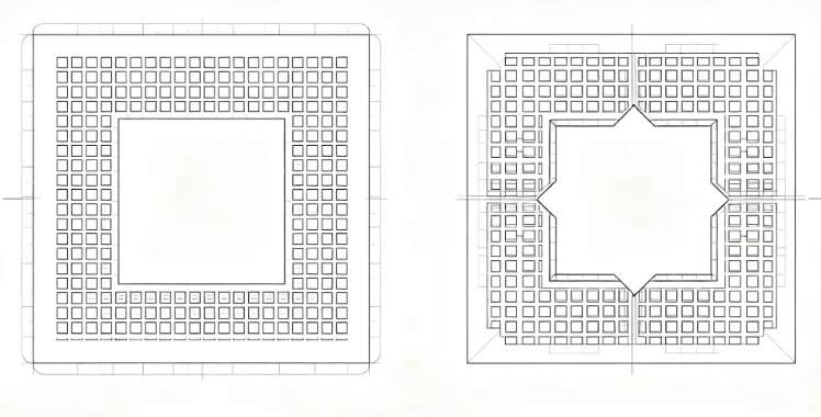
Paste release depends on the balance between the opening area of the aperture and the surface area of its walls. In laser cut stencils, the cutting process creates relatively smooth vertical walls that reduce adhesion compared to etched alternatives. Modified aperture shapes alter this balance further by adjusting the perimeter or introducing tapers that facilitate cleaner separation from the stencil during the print cycle.
For BGA components, aperture design often incorporates reductions or shape changes to control the exact volume of paste deposited on each pad. This prevents excess material that could cause shorts while ensuring enough paste remains after reflow for reliable joints. Area ratio calculations, as outlined in relevant standards, help determine whether a given aperture will release paste effectively under typical printing pressures and speeds.
Related Reading: Advanced Stencil Aperture Designs for Optimized Solder Paste Deposition
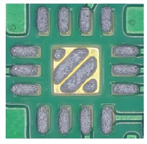
QFN packages present different demands due to their exposed thermal pads. Here, aperture designs frequently segment the opening into multiple smaller sections rather than one large rectangle. This segmentation creates pathways for volatiles to escape during reflow and reduces the risk of large voids under the component. The smooth walls from laser cutting support consistent fill and release even in these divided patterns.
Practical Solutions and Best Practices for Aperture Modification
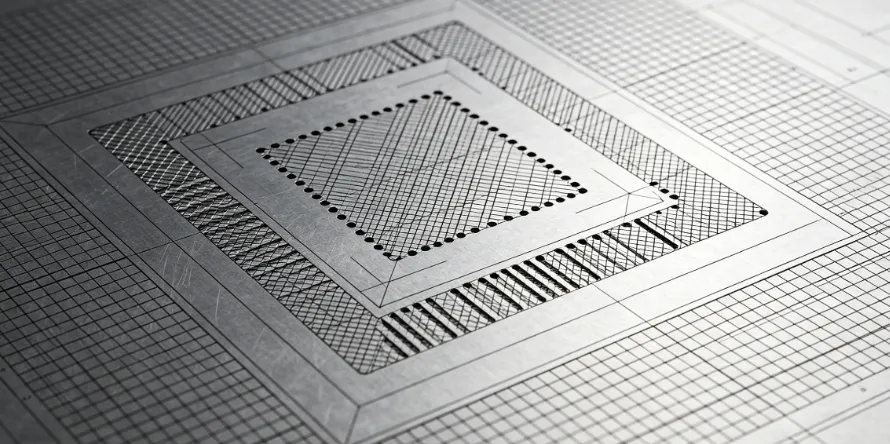
Engineers begin by evaluating component specifications and board layout constraints before selecting aperture shapes. For BGA applications, modified shapes such as home-plate or rounded configurations often improve release from small openings by minimizing sharp corners where paste can cling. These adjustments are applied selectively, typically only to the finest pitch arrays where standard rectangles prove inadequate.
In QFN designs, best practices include using segmented apertures sized to achieve target paste coverage on thermal pads while leaving gaps for outgassing. Laser cut stencils benefit from these modifications because their fabrication precision allows tight control over the resulting geometries. Process parameters like squeegee pressure and print speed are then tuned in conjunction with the aperture design to maximize transfer efficiency.
Troubleshooting common issues starts with print inspection data. Insufficient paste on BGA pads may indicate an area ratio below recommended thresholds, prompting a shift to modified shapes. For QFN thermal pads, bridging or excessive volume often signals the need for further segmentation or slight reductions in overall aperture area. Iterative testing on production-like boards validates each change before full-scale implementation.
Related Reading: The Art of SMT Stencil Aperture Design: Minimizing Defects and Maximizing Yield
Troubleshooting Insights from Assembly Processes
When defects appear, systematic review of aperture performance reveals root causes. Bridging between BGA balls frequently traces back to oversized or poorly shaped apertures that deposit excess paste. Adjusting to modified shapes with controlled reductions restores separation between deposits without sacrificing joint strength.
Paste release failures on QFN packages often stem from large single apertures that retain material on the walls. Switching to segmented patterns, combined with the inherent advantages of laser cut smoothness, typically resolves these problems. Monitoring environmental factors such as paste viscosity and ambient temperature during printing further supports consistent results across batches.
These targeted adjustments align with established industry practices for maintaining high yields in mixed-component assemblies.
Conclusion
Advanced aperture design techniques for laser cut stencils enable reliable solder paste application on challenging components like BGAs and QFNs. By focusing on paste release through modified shapes and segmented patterns, engineers achieve better process control and fewer defects. Reference to standards such as IPC-7525 ensures these methods remain grounded in proven guidelines. Continued attention to these details supports consistent assembly quality as component complexity increases.
FAQs
Q1: What considerations guide aperture design for BGA components?
A1: Aperture design for BGA focuses on achieving precise paste volumes on small pads while preventing bridging. Modified shapes help improve release from laser cut stencils, and designs follow area ratio recommendations in IPC-7525 to support consistent transfer.
Q2: How does aperture design for QFN differ from standard approaches?
A2: Aperture design for QFN often uses segmented patterns on thermal pads to manage volume and allow volatile escape. This approach, suited to laser cut stencil characteristics, reduces voiding risks compared to single large openings.
Q3: Why is laser cut stencil paste release important in fine-pitch applications?
A3: Laser cut stencil paste release determines whether solder paste transfers cleanly to the board without residue on aperture walls. Effective release becomes critical for small apertures in BGA and QFN designs to avoid insufficient joints or defects.
Q4: When should modified aperture shapes be considered?
A4: Modified aperture shapes are considered when standard rectangles fail to deliver adequate release or volume control on fine-pitch or thermal-pad components. Evaluation against paste release metrics and standards like IPC-7525 informs the decision.
References
IPC-7525C — Stencil Design Guidelines. IPC, 2021
J-STD-001H — Requirements for Soldered Electrical and Electronic Assemblies. IPC, 2020