 ALLPCB


Introduction
Trace width plays a pivotal role in printed circuit board design and production, influencing everything from electrical performance to overall PCB manufacturing cost. Engineers often prioritize compact layouts with narrow traces to maximize component density, yet this choice can significantly elevate fabrication expenses. Factories must employ advanced imaging and etching techniques for finer features, which demand specialized equipment and stricter process controls. Understanding trace width tolerances and minimum trace width requirements helps balance functionality with economic viability. This article explores how trace width decisions affect costs, drawing on factory insights and design for manufacturability principles. By optimizing trace widths, teams can reduce PCB manufacturing costs without compromising reliability.
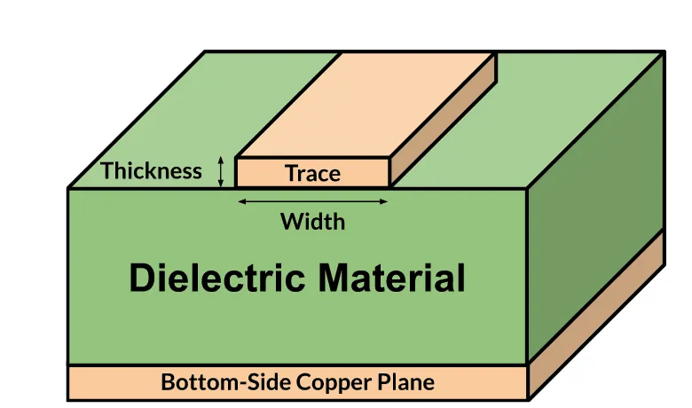
Understanding Trace Width and Its Relevance in PCB Production
Trace width refers to the lateral dimension of copper conductors on a PCB, critical for carrying current, managing heat, and maintaining signal integrity. Standards like IPC-2221 provide guidelines for determining appropriate widths based on current load and temperature rise, ensuring safe operation. In manufacturing, trace width tolerances define the allowable deviation from design specifications, typically tighter for high-density boards. Minimum trace width sets the fabrication limit, below which processes become unreliable and costly. These factors directly tie into PCB manufacturing cost because narrower traces require higher resolution in photolithography and etching steps. Factory experience shows that adhering to standard tolerances improves yield and lowers expenses.
Deviating from standard trace widths complicates production workflows. For instance, excessive narrowing reduces etch margins, increasing defect risks like opens or shorts. Conversely, overly wide traces may underutilize panel space, raising material costs per board. Design for manufacturability emphasizes selecting widths that align with fab capabilities, avoiding premiums for exotic processes. Engineers must consider class levels in standards, where Class 2 boards tolerate looser specs than Class 3. Ultimately, informed trace width choices drive cost efficiency across production volumes.
How Trace Width Affects Key Manufacturing Processes
The imaging stage kicks off trace formation, where photoresist coats the copper foil before exposure defines the pattern. Narrower traces demand higher resolution exposure systems, often shifting from traditional film to laser direct imaging for precision. This upgrade alone inflates setup times and equipment depreciation in PCB manufacturing cost calculations. Etching follows, dissolving unwanted copper; finer features require controlled etchants to prevent undercutting, which narrows traces beyond tolerances. Factories monitor etch factors closely, as imbalances lead to yield losses that amplify per-unit costs.
Plating and surface finishing add layers of complexity for narrow traces. In multilayer boards, vias and traces interact, where minimum trace width tolerances ensure isolation. Advanced processes like electrolytic plating for heavy copper demand uniform deposition, harder with tight geometries. Inspection steps intensify too, using automated optical systems to verify widths against specs like those in IPC-A-600. Non-conformances trigger rework or scrap, directly hiking PCB manufacturing cost. Process engineers optimize chemistry and conveyor speeds for standard widths, achieving higher throughput.
Panel utilization ties trace width to economies of scale. Dense patterns with fine traces allow more boards per panel, potentially offsetting costs through volume. However, defect propagation across panels erodes this advantage, especially if minimum trace width pushes limits. Factories apply design for manufacturability rules to predict routability and spacing. Thermal management during lamination also factors in, as trace density affects resin flow and voiding. Overall, these interconnected processes reveal why trace width optimization is factory-critical.
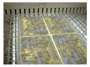
Trace Width Tolerances and Their Cost Implications
Trace width tolerances specify production variability, often expressed as percentages of nominal design. Looser tolerances suit standard runs, enabling faster cycles and lower PCB manufacturing cost. Tighter specs for high-frequency boards necessitate metrology tools and statistical process control, adding overhead. IPC-6012 outlines performance qualifications where conductor widths must meet minimum thresholds for reliability. Factories calibrate equipment to these, with deviations triggering lot rejections.
Cost escalates nonlinearly with tightening tolerances. Standard external trace tolerances allow for natural etch bias, keeping processes economical. Demanding sub-micron control invokes cleanroom protocols and premium resists, reserved for HDI boards. Yield modeling predicts cost curves: a 20 percent reduction in minimum trace width might double defect rates in volume production. Design for manufacturability urges specifying achievable tolerances upfront. Procurement teams benefit by quoting based on fab DFM feedback, avoiding surprises.
Internal layers pose unique challenges due to sequential lamination. Trace width tolerances here suffer from registration errors, compounding costs in multilayer stacks. Factories use X-ray inspection for buried features, a step omitted in simpler designs. Adhering to class-defined tolerances per IPC standards minimizes these extras. Engineers gain by simulating tolerances early, aligning design with fab realities.
Design for Manufacturability: Optimizing Trace Width for Cost Savings
Effective design for manufacturability starts with IPC-2221 guidelines for current-carrying capacity, dictating minimum trace width without excess narrowing. Engineers calculate widths accounting for copper weight and rise temperatures, padding for tolerances. Standard signal traces benefit from 6 to 10 mil widths in many fabs, balancing density and cost. Power traces widen naturally for ampacity, rarely driving up expenses.
Spacing rules complement trace width, as minimum clearances prevent bridging during etching. Factories recommend 1:1 trace-to-space ratios for standard processes, easing imaging alignment. Violating this invites impedance mismatches and rework fees. Layer stackup influences too; thinner dielectrics amplify field effects, necessitating wider traces for isolation. DFM checklists include annuli and pad sizing, holistic to trace optimization.
Software aids by flagging violations pre-tapeout. Factories provide capability matrices outlining cost tiers by minimum trace width. Prototypes validate assumptions, refining production designs. Collaborative reviews between design and fab teams catch issues early. Such practices routinely cut PCB manufacturing cost by 15 to 30 percent through yield gains.

Cost Breakdown: Quantifying Trace Width's Financial Impact
Material costs rise modestly with finer traces due to resist and chemistry premiums. However, equipment amortization dominates: high-res imagers cost millions, spreading over standard volumes. Labor intensifies for handling and inspection of dense patterns. Yield directly multiplies these, with narrow traces prone to systematic defects like mouse bites.
Setup and tooling fees scale with complexity. Photoplot changes for each width variant add charges. NRE for fine-line processes includes test panels and profiling. Volume pricing tiers reward standard minimum trace widths, with premiums for below-threshold specs. High-mix low-volume runs suffer most from trace variability.
Post-etch metrology and electrical testing verify tolerances. Failures cascade to assembly delays, inflating total ownership costs. Factories mitigate via process windows tailored to design rules. Procurement analyzes quotes dissecting line width impacts. Long-term, standardizing on achievable tolerances stabilizes supply chains.
Practical Insights from Factory Production Floors
In high-volume runs, boards with uniform trace widths achieve panel efficiencies above 90 percent. Finer minimum trace widths drop this, as edge effects waste real estate. Factories segment lines by capability: standard for 5 mil plus, advanced for tighter. Cross-training operators maintains flexibility without cost spikes.
Multilayer alignment challenges narrow traces, where via capture demands precise registration. IPC-A-600 criteria guide visual accepts, training inspectors consistently. Yield analytics track trace-related fails, feeding back to DFM. Engineers iterate designs post-prototype, widening non-critical nets.
Sustainability angles emerge: finer processes consume more energy and waste. Broader traces enable simpler chemistries, aligning with green initiatives. Factory data underscores design for manufacturability as the cost lever.
Conclusion
Trace width profoundly shapes PCB manufacturing cost through process demands, yield, and efficiency. Adhering to standards like IPC-2221 and IPC-A-600 ensures reliable, economical production. Prioritizing design for manufacturability with realistic tolerances and minimum trace widths optimizes outcomes. Engineers balancing density and cost gain competitive edges. Factories thrive on collaborative designs, minimizing premiums. Ultimately, informed trace decisions deliver high-performance boards at sustainable prices.
FAQs
Q1: What factors determine minimum trace width in PCB design?
A1: Minimum trace width depends on current capacity, thermal limits, and fab capabilities, as guided by IPC-2221. Factories recommend padding for etch tolerances to ensure manufacturability. Narrower widths suit high-density needs but raise PCB manufacturing cost due to precision etching. Design for manufacturability tools calculate optimal sizes, preventing over-specification.
Q2: How do trace width tolerances affect PCB manufacturing cost?
A2: Tolerances dictate process controls; standard ±10–20 percent keeps costs low via conventional equipment. Tighter specs demand advanced metrology and slower cycles, inflating expenses. IPC-A-600 defines acceptability classes influencing these. Optimizing tolerances enhances yield, directly lowering per-unit PCB manufacturing cost. Factories advise quoting based on specified classes.
Q3: Why is design for manufacturability crucial for trace width?
A3: Design for manufacturability aligns trace widths with fab limits, avoiding premiums for fine features. It incorporates IPC guidelines for current and spacing, maximizing panel yield. Poor choices lead to defects and rework, hiking costs. Early DFM reviews ensure cost-effective minimum trace widths without performance trade-offs.
Q4: Can wider traces always reduce PCB manufacturing cost?
A4: Wider traces simplify etching and boost yield in standard processes, often cutting costs. However, they increase material use and may limit density. Balance via IPC-2221 for ampacity ensures efficiency. Factories favor them for high-volume production, where tolerances are easier to hold.
References
IPC-2221B — Generic Standard on Printed Board Design. IPC, 2003
IPC-A-600K — Acceptability of Printed Boards. IPC, 2020
IPC-6012E — Qualification and Performance Specification for Rigid Printed Boards. IPC, 2015





