ALLPCB



Embedded component technology integrates passive and active devices directly into the layers of a printed circuit board. This approach reduces overall board size while improving electrical performance and mechanical reliability. Advanced PCB materials play a central role in enabling these designs by providing the necessary electrical, thermal, and mechanical properties. Engineers increasingly evaluate PCB substrate selection based on application requirements such as operating frequency, power dissipation, and environmental conditions. The result is more compact systems that maintain signal integrity and thermal stability under demanding conditions.
Why Advanced Materials Matter for Embedded Component PCBs
Embedded components require PCB materials that support high-density interconnects while surviving multiple lamination cycles and subsequent assembly processes. Traditional FR-4 laminates often fall short when designs demand lower dielectric constants or better thermal conductivity. High-frequency laminates address signal integrity needs in RF and microwave applications by minimizing insertion loss and controlling impedance. Ceramic substrates offer superior heat spreading for power electronics, and flexible substrates enable three-dimensional form factors in wearable or automotive modules. Proper PCB substrate selection therefore directly influences yield, long-term reliability, and overall system performance.
Technical Principles of Key Material Categories
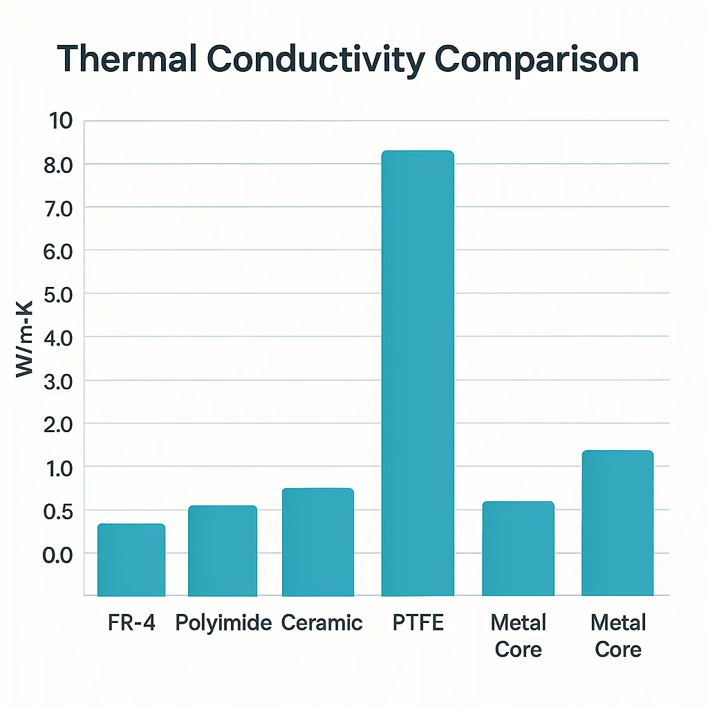
High-frequency laminates typically incorporate hydrocarbon or fluoropolymer resins reinforced with glass or ceramic fillers. These formulations deliver dielectric constants between 2.2 and 3.5 and loss tangents below 0.005 at gigahertz frequencies, supporting controlled impedance routing around embedded components. The low coefficient of thermal expansion in the z-axis helps maintain via integrity during thermal cycling. Ceramic substrates such as alumina or aluminum nitride provide thermal conductivities from 20 to 170 W/m·K, far exceeding organic laminates. Their high modulus and matched expansion characteristics reduce stress on embedded dies during temperature excursions. Flexible substrates based on polyimide films maintain flexibility down to thicknesses of 25 micrometers while offering continuous operating temperatures above 200 °C. When combined with low-flow prepregs, these materials allow components to be embedded without excessive resin squeeze-out that could create voids or delamination.
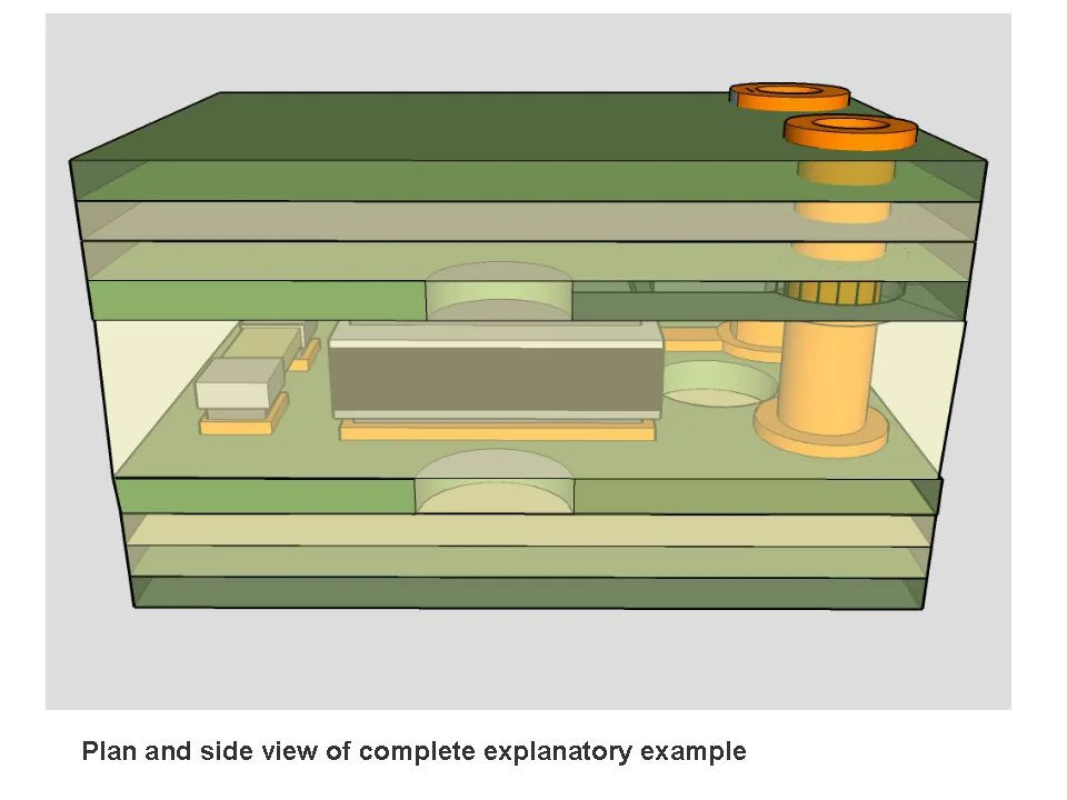
Thermal management becomes critical once components are buried inside the stack-up. Heat generated by embedded active devices must conduct through surrounding dielectric layers to external heat sinks or copper planes. Materials with higher thermal conductivity reduce junction temperatures and extend operating life. Dielectric constant stability across temperature and frequency ranges also prevents drift in filter or resonator performance. Engineers therefore compare material data sheets for glass transition temperature, decomposition temperature, and moisture absorption rates before finalizing PCB substrate selection.
Related Reading: Thermal Management Breakthrough: Using Embedded Components for Efficient PCB Cooling
Best Practices in PCB Substrate Selection and Design
Begin the selection process by defining electrical requirements such as maximum operating frequency and acceptable insertion loss. High-frequency laminates are preferred when signals exceed 1 GHz, while standard high-Tg FR-4 may suffice for lower-speed digital circuits. Next, assess thermal demands by calculating power dissipation and required thermal resistance. Ceramic substrates or metal-core constructions become candidates when power densities exceed 5 W/cm2. Mechanical considerations include flexural strength for flexible substrates and coefficient of thermal expansion matching to prevent warpage or cracking around embedded parts.
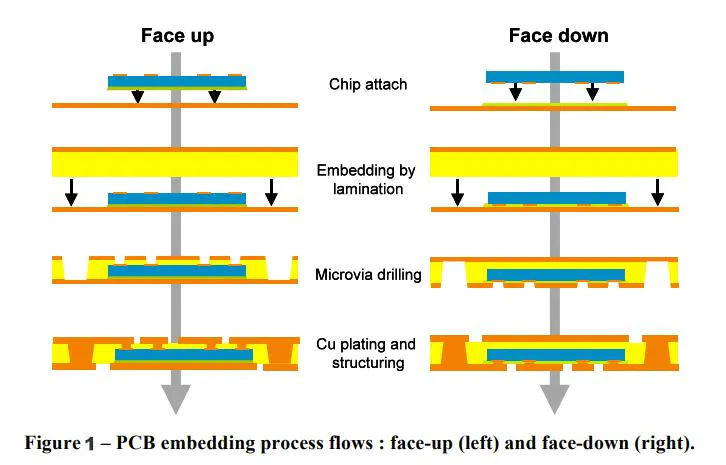
Process compatibility must also be verified. Embedded component flows involve additional lamination steps at temperatures often above 180 °C and pressures up to 400 psi. Materials should exhibit low resin flow and high dimensional stability to avoid shifting of embedded components. Moisture sensitivity is another factor; materials with low moisture absorption reduce the risk of delamination during reflow. JEDEC J-STD-020E provides classification guidelines that help qualify both the board and embedded devices for assembly conditions.
Design rules should account for the different etch factors and via formation methods associated with each material family. High-frequency laminates may require laser drilling or plasma etching for microvias, while ceramic substrates often use thick-film or thin-film metallization. Early collaboration between design and manufacturing teams ensures that stack-up choices support both electrical performance and producibility.
Related Reading: The Future of PCBs: Exploring Advanced Applications of Embedded Component Technology
Conclusion
Advanced PCB materials expand the possibilities for embedded component technology by delivering tailored electrical, thermal, and mechanical properties. High-frequency laminates preserve signal integrity, ceramic substrates manage heat, and flexible substrates enable novel form factors. Systematic PCB substrate selection based on application requirements, combined with adherence to established qualification standards such as IPC-6012E, leads to reliable, high-performance boards. Engineers who understand these material characteristics can design more compact and efficient electronic systems that meet evolving market demands.
FAQs
Q1: What PCB materials are best suited for high-frequency embedded component designs?
A1: High-frequency laminates with low dielectric constant and low loss tangent provide the signal integrity required for RF and microwave circuits containing embedded passives. These materials maintain stable impedance around buried components and reduce insertion loss at gigahertz frequencies. Selection should also consider thermal expansion characteristics to ensure via reliability after lamination.
Q2: How do ceramic substrates improve thermal performance in embedded PCBs?
A2: Ceramic substrates conduct heat away from embedded active devices more effectively than organic laminates, lowering junction temperatures and improving long-term reliability. Their high modulus and controlled expansion also minimize mechanical stress during thermal cycling. Engineers evaluate thermal conductivity values and coefficient of thermal expansion when performing PCB substrate selection for power applications.
Q3: Why is PCB substrate selection critical for flexible embedded component boards?
A3: Flexible substrates such as polyimide must withstand repeated bending while protecting embedded components from strain. Proper material choice ensures adhesion during lamination and maintains electrical performance after flexing. Low moisture absorption and high continuous operating temperature further support reliability in dynamic environments.
Q4: What role do industry standards play in qualifying materials for embedded PCBs?
A4: Standards such as IPC-A-600K define acceptability criteria for the finished board, including embedded features, while JEDEC J-STD-020E classifies moisture sensitivity for assembly. Following these guidelines helps ensure consistent quality and reduces the risk of defects related to material or process variations.
References
IPC-6012E — Qualification and Performance Specification for Rigid Printed Boards. IPC, 2017
IPC-A-600K — Acceptability of Printed Boards. IPC, 2020
JEDEC J-STD-020E — Moisture/Reflow Sensitivity Classification. JEDEC, 2014