 ALLPCB


Introduction
Power distribution network (PDN) design forms the backbone of reliable operation in any printed circuit board, particularly in double-layer PCBs where space constraints amplify challenges. In these boards, engineers must deliver stable voltage and current to components while minimizing noise and losses across just two copper layers. Effective PDN design ensures PCB power integrity, preventing issues like voltage droops that can cause system failures in applications from consumer electronics to industrial controls. Double-layer configurations demand careful planning to mimic the low-impedance paths typically provided by dedicated planes in multilayer boards. This article explores best practices tailored for electric engineers working with power distribution PCBs, drawing on established engineering principles to optimize performance.
What Is a Power Distribution Network in Double-Layer PCBs?
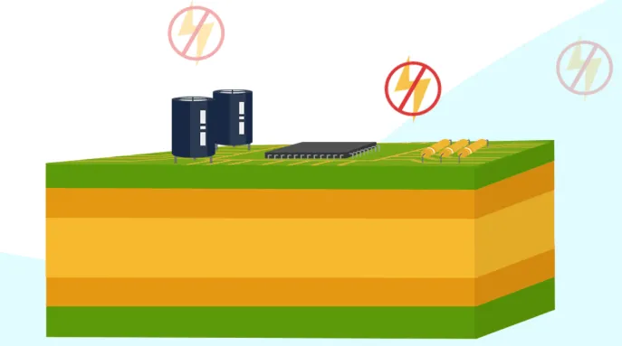
A power distribution network encompasses all conductive paths, from power entry points to component loads, including traces, pours, vias, and decoupling capacitors. In double-layer PCBs, the PDN relies heavily on wide traces and ground pours rather than full planes, as inner layers are absent. This setup distributes DC power while handling transient currents from switching components like microcontrollers or drivers. Key goals include low DC resistance for minimal voltage drop and low AC impedance to suppress noise across frequencies. Poor PDN design leads to hotspots, electromagnetic interference, and unreliable operation, making it critical for double layer PCB power management.
The relevance intensifies in cost-sensitive projects where double-layer boards suffice for moderate complexity. Engineers face trade-offs between routing density and power delivery efficiency. Adhering to guidelines like those in IPC-2221 helps maintain clearances and material choices that support robust PDN performance. Ultimately, a well-designed PDN enhances overall PCB power integrity, extending component lifespan and ensuring compliance with operational specs.
Technical Principles of PDN Design in Double-Layer PCBs
At its core, PDN performance hinges on controlling impedance at both DC and AC levels. DC resistance, governed by trace length, width, and copper thickness, causes IR drops that reduce voltage at loads. For instance, longer paths increase losses, demanding wider traces to handle current without excessive heating. AC impedance arises from inductance in loops formed by power and return paths, amplifying noise during transients. In double-layer boards, overlapping signals or poor ground returns exacerbate this, leading to crosstalk and ripple.
Target impedance defines an upper limit for PDN response, calculated as Vdd / (I * ripple tolerance), guiding capacitor and trace optimization. Return paths must remain continuous and proximate to power traces to minimize loop inductance. Vias introduce additional resistance and inductance, so strategic placement via stitching connects pours effectively. Thermal effects compound issues, as current density raises temperatures, further degrading resistance per IPC-2152 principles for current-carrying capacity.
Ground bounce occurs when simultaneous switching draws current, creating voltage fluctuations across the PDN. Decoupling capacitors provide local charge reservoirs, shunting high-frequency noise to ground. In double-layer setups, the absence of adjacent planes limits plane capacitance, shifting reliance to discrete components and trace geometry.
Best Practices for PDN Design in Double-Layer PCBs
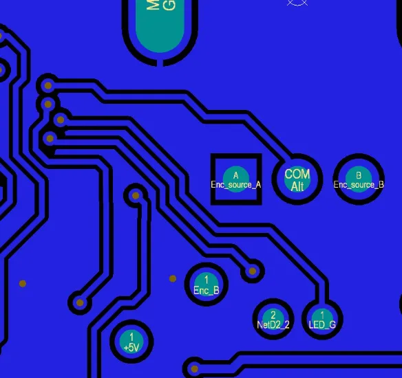
Assign one layer predominantly to ground pours, filling unused areas with copper connected via stitching vias every few millimeters. This creates a low-impedance return plane, reducing EMI and providing reference for signals. On the power layer, route wide traces for distribution, sizing them according to current requirements to limit temperature rise. Follow IPC-2152 for determining trace widths, ensuring safe operation under expected loads without specific numerical fabrication here.
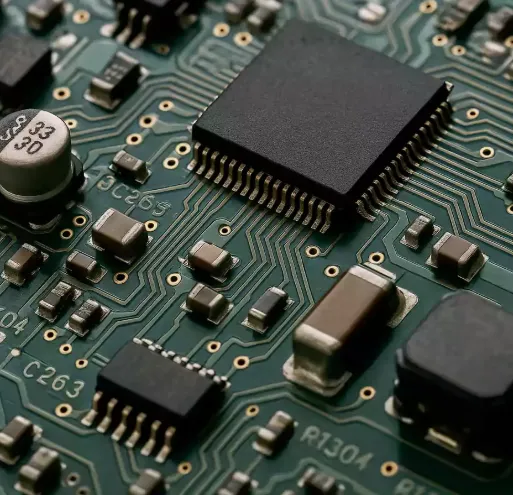
Place decoupling capacitors as close as possible to IC power pins, ideally within 1-2 mm, using a mix of values like 0.1 μF ceramics for high frequencies and larger electrolytics for bulk storage. Connect them with short, wide traces or direct via-in-pad to minimize inductance. For multiple power rails, employ star-point distribution from the entry to avoid ground shifts between branches. Orthogonal routing on layers prevents signal overlap with power lines, curbing crosstalk.
Utilize thicker copper weights, such as 2 oz, for power traces to boost current capacity and reduce resistance. Multiple parallel vias under power entry points share current, lowering overall impedance. Avoid splits in ground pours that could island sections, forcing erratic returns. Simulate PDN impedance profiles early to identify resonances, adjusting capacitor networks accordingly.
Minimize loop areas by routing power and ground traces adjacently where feasible, forming transmission lines with controlled characteristic impedance. For high-current sections, incorporate thermal reliefs on pads to aid soldering while dissipating heat. These practices collectively enhance PCB power integrity in resource-limited double-layer designs.
Common Challenges and Troubleshooting in Double-Layer PDN
Voltage drops plague long power runs, manifesting as dim LEDs or IC resets. Measure drops with scopes at loads under max current, then widen traces or add local regulators. Noise from switching manifests as jitter; probe ripple at pins and add targeted decoupling if exceeding 5% Vdd. Hotspots indicate undersized traces; infrared imaging reveals them, prompting redesign per current guidelines.
Via bottlenecks occur in dense areas, increasing resistance. Replace singles with arrays and larger diameters. Ground loops from poor stitching cause hum; dense via fences resolve this. Warpage from asymmetric copper distorts traces; balance pours across layers. Troubleshooting involves iterative prototyping, as simulations approximate real parasitics.
Conclusion
Mastering PDN design in double-layer PCBs demands disciplined trace sizing, ground pour strategies, and decoupling placement to uphold power integrity. These practices mitigate impedance issues inherent to limited layers, ensuring stable delivery amid constraints. Electric engineers benefit from logical adherence to principles like low-loop inductance and balanced returns. Prioritizing simulation and verification yields robust power distribution PCBs suitable for diverse applications. Implementing these best practices elevates design reliability without escalating to multilayer complexity.
FAQs
Q1: What role do ground pours play in double layer PCB power distribution?
A1: Ground pours on both layers provide low-impedance returns, essential for PDN design in double-layer boards lacking dedicated planes. They suppress EMI by shortening return paths and stabilize reference voltages. Stitch pours with vias spaced closely to prevent islands. This approach enhances PCB power integrity, reducing noise coupling to signals. Follow layout symmetry to avoid warpage.
Q2: How do you size traces for power distribution PCB currents?
A2: Trace widths depend on current, copper thickness, and allowable temperature rise, guided by IPC-2152 standards. Wider traces lower resistance and heating in high-current paths. Use 2 oz copper for demanding sections and parallel paths for sharing. Verify with thermal simulations to prevent hotspots. Proper sizing ensures reliable double layer PCB power delivery.
Q3: Why is decoupling critical for PDN design in double-layer PCBs?
A3: Decoupling capacitors supply transient currents, maintaining low AC impedance in PDN networks without plane capacitance. Place them near loads with mixed values covering frequency ranges. Short connections minimize ESL, curbing voltage droops. In double-layer setups, they compensate for higher inductance. This preserves PCB power integrity during switching events.
Q4: What are common PDN pitfalls in double-layer boards?
A4: Overlapping power and signals induces noise, while long traces cause drops. Undersized vias bottleneck current, and unbalanced pours lead to warpage. Mitigate with orthogonal routing, stitching, and simulations. Adhering to IPC-2221 clearances prevents breakdowns. Early prototyping identifies issues for refined power distribution PCB performance.
References
IPC-2221C — Generic Standard on Printed Board Design. IPC, 2017
IPC-2152A — Standard for Determining Current Carrying Capacity in Printed Board Design. IPC, 2009
IPC-6012E — Qualification and Performance Specification for Rigid Printed Boards. IPC, 2017





